Epitaxial wafer including nitride-based semiconductor layers

A nitride-based, epitaxial wafer technology, applied in the field of epitaxial wafers, can solve the problems of reduced edge dislocation density, cracks, and no crystallinity improvement effect, and achieve the effect of reducing the edge dislocation density

Inactive Publication Date: 2013-01-23
SHARP KK
View PDF9 Cites 16 Cited by
  • Summary
  • Abstract
  • Description
  • Claims
  • Application Information

AI Technical Summary

Problems solved by technology

[0012] Moreover, regarding the composition gradient buffer layer structure, as according to Figure 4 As predicted, with the increase of the total thickness, the edge dislocation density in the GaN channel layer may be further reduced, but there is an increase in the warpage of the wafer with the increase of the composition gradient buffer layer structure thickness, thus The subject of cracks
[0013] In addition, even in a structure that combines a multilayer buffer layer and a composition gradient buffer layer, depending on how the multilayer buffer layer and composition gradient buffer layer are combined, there may be a problem that the crystallinity improvement effect may not be exhibited at all.

Method used


Image

  • Epitaxial wafer including nitride-based semiconductor layers
  • Epitaxial wafer including nitride-based semiconductor layers
  • Epitaxial wafer including nitride-based semiconductor layers

Examples


no. 1 example )

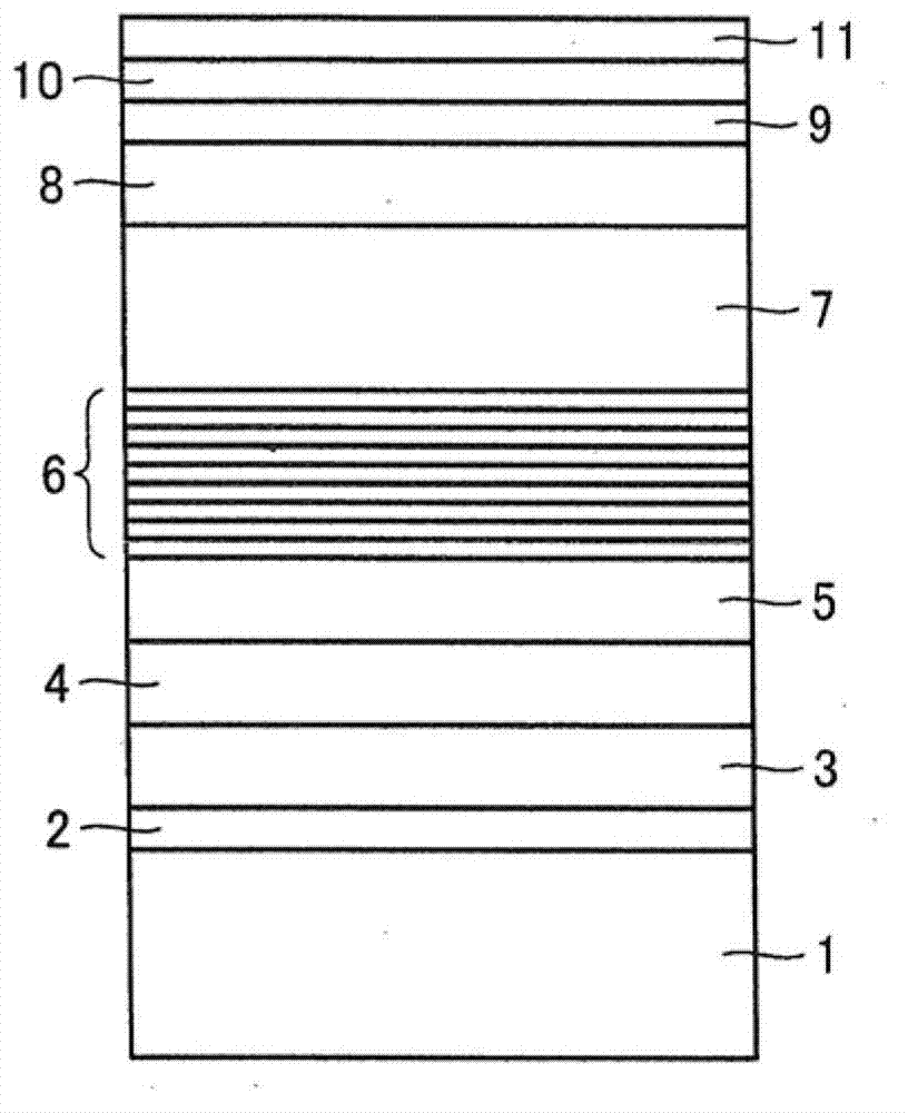
[0039] figure 1 is a schematic cross-sectional view of an epitaxial wafer applied to a heterojunction field effect transistor showing the first embodiment of the present invention.

[0040] In the production of this wafer, a Si substrate 1 with a diameter of 4 inches was used as the substrate. Before the crystal growth of the nitride-based semiconductor layer, the surface oxide film of the Si substrate 1 is removed by a hydrofluoric acid-based etchant, and then the substrate is set in a chamber of an MOCVD (Metal Organic Chemical Vapor Deposition) apparatus.

[0041] The substrate was heated to 1100° C. in the MOCVD apparatus, and the surface of the substrate was cleaned in a hydrogen environment with a pressure of 13.3 kPa in the chamber.

[0042] Afterwards, by maintaining the substrate temperature and chamber pressure, and flowing NH 3 (12.5slm), the surface of the Si substrate is nitrided. Next, at TMA (trimethylaluminum) flow = 117 μmol / min and NH 3 Under the conditi...


PUM


Abstract

An epitaxial wafer including nitride-based semiconductor layers usable for a hetero-junction field effect type transistor, includes a first buffer layer of AlN or AlON, a second buffer layer of AlxGa1-xN having its Al composition ratios decreased in a stepwise fashion, a third buffer layer including a multilayer of repeatedly stacked AlaGa1-aN layers / AlbGa1-bN layers disposed on the second buffer layer, a GaN channel layer, and an electron supply layer in this order on a Si substrate, wherein the Al composition ratio x in the uppermost part of the second buffer layer is in a range of 0!<=x!<=0.3.

Description

technical field [0001] The present invention relates to an epitaxial wafer comprising a plurality of layers of nitride-based semiconductors belonging to III-V group compound semiconductors, and in particular to improvement of warp and crystallinity of an epitaxial wafer capable of being used for a heterojunction field effect transistor. It should be noted that it is known that a two-dimensional electron gas can be generated at the heterojunction interface of such a nitride-based semiconductor epitaxial wafer. Background technique [0002] For example, in the case of fabricating an epitaxial wafer including a heterojunction formed of a GaN channel layer and an AlGaN barrier layer, which can be used in a heterojunction field effect transistor, the high price of the GaN substrate currently makes all The nitride semiconductor layer is crystal-grown on substrates of different materials such as sapphire or Si. [0003] In the case of growing a nitride-based semiconductor layer on...

Claims


Application Information

Patent Timeline
Patent Type & Authority Applications(China)
IPC IPC(8): H01L29/778H01L29/10
CPCH01L29/7787H01L21/02381H01L29/207H01L21/02458H01L21/0262H01L29/778H01L21/02488H01L29/2003H01L29/10H01L21/02507H01L29/66462H01L21/0254
Inventor 寺口信明本田大辅伊藤伸之矢仓基次
Owner SHARP KK
Why Eureka
Try Eureka