Random mesh design method of metal net conductive thin film, conductive film and manufacturing method of conductive film

A technology of random mesh and conductive film, applied in cable/conductor manufacturing, conductive layer on insulating carrier, circuit, etc., can solve the problems of Moiré fringe transmittance and difference, and avoid the generation of moiré fringes. Effect

Inactive Publication Date: 2013-01-30
SUZHOU INST OF NANO TECH & NANO BIONICS CHINESE ACEDEMY OF SCI
View PDF6 Cites 33 Cited by
  • Summary
  • Abstract
  • Description
  • Claims
  • Application Information

AI Technical Summary

Problems solved by technology

[0007] In view of this, the object of the present invention is to provide a random grid design method of a metal mesh conductive film,

Method used


Image

  • Random mesh design method of metal net conductive thin film, conductive film and manufacturing method of conductive film
  • Random mesh design method of metal net conductive thin film, conductive film and manufacturing method of conductive film
  • Random mesh design method of metal net conductive thin film, conductive film and manufacturing method of conductive film

Examples


Embodiment 1

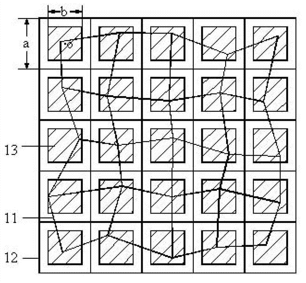
[0047] In this embodiment, the type of random grid is a trapezoidal grid, such as figure 1 11 in. First, a rectangular coordinate system is established in a two-dimensional plane space, and a square 12 is drawn in the rectangular coordinate system. The coordinates of the four vertices of the square 12 are (0,0), (a,0), (a,a), (0, a), the squares 12 are arrayed in a two-dimensional plane, and the periods along the x and y directions are a , to form a regular grid of squares; then define an effective area within each square that can generate random points, the center of the effective area and the center of the square o same as figure 1 Shown in the shaded area 13 in , and generate random points in the effective area 13, the effective area is also a square in this embodiment, and the side length isb ; Finally, connect random points inside the same row of squares, and connect random points inside the same column of squares to form a random grid composed of trapezoids. Based on ...

Embodiment 2

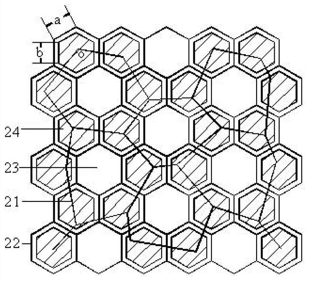
[0049] In this embodiment, the type of random grid is an irregular hexagonal grid, such as figure 2 21 in. Similar to Embodiment 1, first establish a rectangular coordinate system in a two-dimensional plane space, draw a regular hexagon 22 in this rectangular coordinate system, and the side length is a , the regular hexagons 22 are arrayed in a two-dimensional plane to form a typical honeycomb grid; then a regular hexagon is selected as the center 23, and random points can be generated by defining inside the six regular hexagons adjacent to the center The effective area of ​​, the center of the effective area and the center of each regular hexagon o Similarly, in this embodiment, the effective area is also a regular hexagon, and the side length is b ,Such as figure 2 As shown in the shaded area 24 in , random points are generated in the effective area 24, and the generated random points are connected clockwise in pairs to form an irregular hexagon; finally, another regula...

Embodiment 3

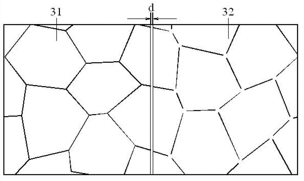
[0051] In this embodiment, the type of the random grid is an irregular hexagonal grid, and the generation method is as described in Embodiment 2. Such as image 3 As shown, the left shaded area is the conductive area 31 of the metal mesh conductive film, and a continuous hexagonal random grid is laid in the area; the right area is the insulating area 32 of the metal mesh conductive film, and the hexagonal grid with disconnected nodes is laid in the area. Random mesh of polygons; width between conductive region 31 and insulating region 32 d Separated by the blank area, so as to achieve electrical isolation. In this example d It is 10μm, which is invisible to the naked eye after testing. Since the grid type and density of the conductive area and the insulating area are exactly the same, that is, the shading ratio of the grid lines in the two areas is the same, so obviously the transmittance is also exactly the same, so there will be no gray scale change. The method of node d...


PUM


Abstract

The invention discloses a random mesh design method of a metal net conductive thin film, comprising the steps of: I. drawing a regular graph in a rectangular coordinate system of a two-dimensional plane space, and periodically arranging the regular graph being as a unit mesh in the two-dimensional plane to form a periodic mesh composed of the unit mesh; II. defining an effective region, capable of generating random points, in the unit mesh in the step I; III. generating the random points in the effective region in the step II; and IV. connecting the random points according to a certain law in the step to form a random mesh composed of the irregular graphs. The invention further discloses a conductive film and a manufacturing method of the conductive film. The core of the random mesh design method is as follows: the random mesh formed by irregular polygons is generated by the periodic mesh formed by the regular graph, so that generation of moire fringes is avoided and transmittance difference is eliminated.

Description

technical field [0001] The invention belongs to the field of conductive films, and in particular relates to a random grid design method of a metal mesh conductive film, a conductive film and a manufacturing method thereof. Background technique [0002] The ITO (Indium tin oxide, indium tin oxide) layer is a crucial part of the touch screen module. Because the traditional process includes ITO coating, ITO patterning, and conductive silver wire production, the production process is cumbersome, so the yield control is difficult, and A large amount of ITO and metal materials will be wasted. Compared with the cumbersome ITO patterning process, using the printing method to directly form a metal grid on a designated area of ​​the substrate can save the patterning process and has many advantages such as low pollution and low cost. With the development trend of ultra-thin and lightweight mobile phone touch screens, flexible patterned metal mesh conductive films are widely used. Jap...

Claims


Application Information

Patent Timeline
IPC IPC(8): G06F17/50H01B5/14H01B13/00
Inventor 高育龙崔铮
Owner SUZHOU INST OF NANO TECH & NANO BIONICS CHINESE ACEDEMY OF SCI
Why Eureka
Try Eureka