
Manufacturing method of pixel structure

A fabrication method and technology of pixel structure, which are applied in semiconductor/solid-state device manufacturing, electrical components, circuits, etc., can solve the problem that the photomask is expensive, the manufacturing cost of the pixel structure 90 cannot be effectively reduced, and the manufacturing cost of the pixel structure 90 cannot be reduced. and other problems, to achieve the effect of low cost

Inactive Publication Date: 2013-01-30
AU OPTRONICS CORP
View PDF2 Cites 2 Cited by
  • Summary
  • Abstract
  • Description
  • Claims
  • Application Information

AI Technical Summary

Problems solved by technology

Since the cost of the photomask is very expensive, and each photomask process must use a photomask with different patterns, if the number of photomask processes cannot be reduced, the manufacturing cost of the pixel structure 90 will not be reduced.
[0006] In addition, as the size of thin film transistor liquid crystal display panels increases, the size of the photomask used to make the thin film transistor array substrate will also increase accordingly, and the large size photomask will be more expensive in cost, making the pixel structure The manufacturing cost of 90 cannot be effectively reduced

Method used


Image

  • Manufacturing method of pixel structure
  • Manufacturing method of pixel structure
  • Manufacturing method of pixel structure

Examples


Embodiment Construction

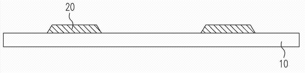
[0052] Figure 2A~Figure 2G It is a schematic diagram of a manufacturing method of a pixel structure of the present invention. Please refer to Figure 2A Firstly, the substrate 200 is provided, and the material of the substrate 200 is, for example, hard or soft materials such as glass and plastic. Next, a first conductive layer 210 is formed on the substrate 200, wherein the first conductive layer 210 is formed by, for example, sputtering, evaporation or other thin film deposition techniques.

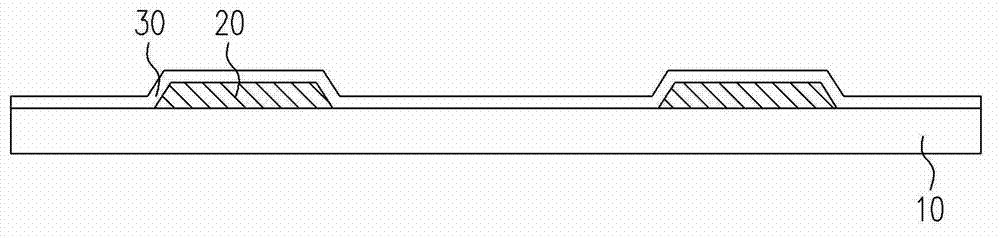
[0053] Next, if Figure 2B As shown, a first mask S1 is provided above the first conductive layer 210 , and the first mask S1 exposes a portion of the first conductive layer 210 , and a laser L is used to irradiate the first conductive layer 210 through the first mask S1 . In detail, the first conductive layer 210 irradiated by the laser L absorbs the energy of the laser L and is ablated from the surface of the substrate 200 . Specifically, the energy of the laser L used to peel off...


PUM

PropertyMeasurementUnit
Wavelengthaaaaaaaaaa

Abstract

The invention relates to a manufacturing method of a pixel structure. The method comprises the following steps of: firstly, providing a substrate on which a first conductive layer is formed, providing a first cover above the first conductive layer, and irradiating the first conductive layer through the first cover by using laser to form a gate; secondly, forming a gate insulating layer on the substrate to cover the gate; thirdly, simultaneously forming a channel layer, a source and a drain on the gate insulating layer above the gate, wherein the gate, the channel layer, the source and the drain form a thin film transistor; fourthly, forming a graphical protection layer on the thin film transistor, wherein the graphical protection layer is exposed from part of the drain; and finally, forming a pixel electrode which is electrically connected to the drain. The gate is manufactured in a laser ablation mode, so manufacturing of the channel layer, the source and the drain can be simultaneously completed. Therefore, compared with a common pixel structure manufacturing method, the manufacturing method of the pixel structure has the advantages that process steps can be simplified, and the manufacturing cost of an optical mask is reduced.

Description

[0001] This application is a divisional application of an invention patent application with a filing date of December 26, 2007, an application number of 200710305314.2, and an invention title of "Method for Making a Pixel Structure". technical field [0002] The present invention relates to a method for manufacturing a pixel structure, and in particular to a method for manufacturing a pixel structure using a laser ablation process to make a protective layer. Background technique [0003] A display is a communication interface between people and information, and flat-panel displays are currently the main development trend. There are mainly the following types of flat panel displays: organic electroluminescence display, plasma display panel, and thin film transistor liquid crystal display. Among them, thin film transistor liquid crystal display is the most widely used. Generally speaking, a thin film transistor liquid crystal display is mainly composed of a thin film transist...

Claims


Application Information

Patent Timeline
IPC IPC(8): H01L21/77
Inventor 方国龙杨智钧黄明远林汉涂石志鸿廖达文詹勋昌蔡佳琪
Owner AU OPTRONICS CORP
Features
  • Generate Ideas
  • Intellectual Property
  • Life Sciences
  • Materials
  • Tech Scout
  • Unparalleled Data Quality
  • Higher Quality Content
  • 60% Fewer Hallucinations
Learn More