Light emitting diode package and method for manufacturing same

A technology for light-emitting diodes and a manufacturing method, which is applied to electrical components, electric solid-state devices, circuits, etc., can solve the difficulty of optical power or brightness and its color rendering, the complex manufacturing process of light-emitting diode units, and the increase in manufacturing costs of light-emitting diode units, etc. problems, to achieve the effect of being conducive to thinning, reducing thickness, and reducing manufacturing costs

Inactive Publication Date: 2013-01-30
斗星A-TECH +1
View PDF3 Cites 6 Cited by
  • Summary
  • Abstract
  • Description
  • Claims
  • Application Information

AI Technical Summary

Problems solved by technology

Therefore, there are problems in that the manufacturing process of the light emitting diode unit is complicated, and the manufacturing cost of the light emitting diode unit is increased.
[0010] In addition, in the prior art, the light-emitting diode chip is mounted on the lead frame and then packaged. Since the light-emitting diode package is mounted on the printed circuit board, therefore, There is the following problem: the thickness of the light emitting diode unit is increased as a whole, so that the thinning of electronic products using the above light emitting diode unit is hindered
[0013] The light-emitting diode unit of the prior art as described above has limitations in improving the wavelength conversion efficiency of emitted light, thereby improving light power or brightness and its color rendering sexually difficult

Method used


Image

  • Light emitting diode package and method for manufacturing same
  • Light emitting diode package and method for manufacturing same
  • Light emitting diode package and method for manufacturing same

Examples


Embodiment Construction

[0039] Hereinafter, preferred embodiments of the light emitting diode package and its manufacturing method according to the present invention will be described in detail.

[0040] The features and advantages of the light emitting diode package and its manufacturing method according to the present invention will be more clearly understood through the detailed description of the following embodiments.

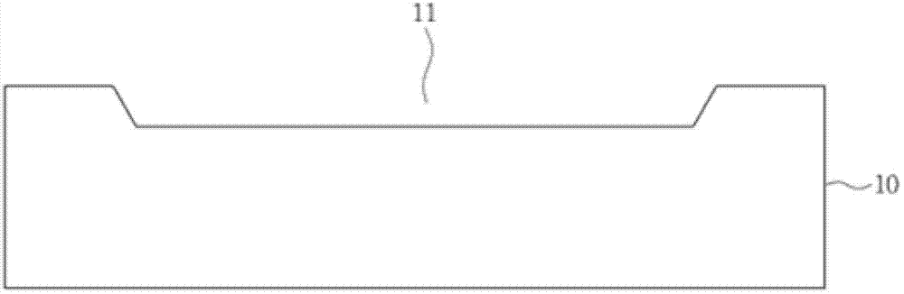
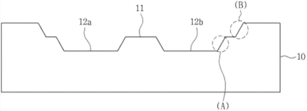
[0041] Figure 1a to Figure 1f is a process cross-sectional view for manufacturing a light emitting diode package according to the present invention, figure 2 is an enlarged structural view of the chip bonding area of ​​the light emitting diode package according to the present invention.

[0042] In the present invention, a heat dissipation substrate with a multi-layer reflective surface is used, and the wiring pattern layer is extended to the lower lower surface of the chip mounting area, thereby ensuring the ease of the chip bonding process and reducing the thickness of the pa...


PUM


Abstract

The invention relates to a light emitting diode package and a method for manufacturing a same, wherein the light emitting diode package uses a heat-dissipating substrate with a plurality of layers of reflectors, and wiring pattern layers are extended to bottom surfaces of a chip mounting area, thereby ensuring easiness of welding technology and reducing thickness of the package. The light emitting diode package includes a heat-dissipating substrate including a reflective groove having a lower bottom surface, an upper opening having a width greater than the lower bottom surface, and an inclined surface formed between the upper opening and the lower bottom surface and mounting grooves, each formed in the reflective groove and having a lower bottom surface, an upper opening having a width greater than the lower bottom surface, and an inclined surface formed between the upper opening and the lower bottom surface; an insulating layer selectively formed on the heat-dissipating substrate; wiring pattern layers formed on the insulating layer and extending to bottom surfaces of the mounting grooves to be selectively formed thereon; a light emitting diode chip mounted in each of the mounting grooves; and a molding layer formed around the light emitting diode chip.

Description

technical field [0001] The present invention relates to the manufacture of a light emitting diode unit, in particular to a light emitting diode package and a manufacturing method thereof, wherein a heat dissipation substrate having a multi-layer reflective surface is used, and the wiring pattern layer is extended to the lower bottom surface of the chip mounting area, thereby ensuring chip bonding Ease of process, and can reduce the thickness of the package. Background technique [0002] Light-emitting diodes use the p-n junction structure of semiconductors to produce injected minority carriers (electrons or holes), and emit light through the recombination of the minority carriers. [0003] Light emitting diodes as described above are used in various fields. Recently, light emitting diodes are attracting attention as components that will replace fluorescent lamps because they have a semi-permanent lifespan and do not contain hazardous substance environmental regulations (RoHS...

Claims


Application Information

Patent Timeline
Patent Type & Authority Applications(China)
IPC IPC(8): H01L33/48H01L33/60H01L33/62H01L33/64H01L33/54
CPCH01L33/48H01L33/60H01L33/642H01L33/64H01L2224/48091H01L2224/73265H01L33/62H01L33/54H01L2924/00014
Inventor 张种镇
Owner 斗星A-TECH
Why Eureka
Try Eureka