Array substrate and display device

An array substrate and substrate technology, applied in optics, instruments, electrical components, etc., can solve problems such as the average LCD brightness difference, and achieve the effect of reducing chromatic aberration and brightness difference.

Active Publication Date: 2013-02-06
BOE TECH GRP CO LTD +1
View PDF5 Cites 24 Cited by
  • Summary
  • Abstract
  • Description
  • Claims
  • Application Information

AI Technical Summary

Problems solved by technology

[0008] The technical problem to be solved by the present invention is: how to further average the brightness difference of liquid crystal display to reduce the color difference

Method used


Image

  • Array substrate and display device
  • Array substrate and display device
  • Array substrate and display device

Examples


Embodiment 1

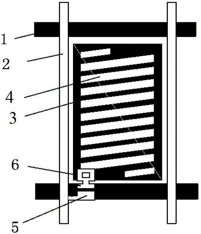
[0038] The array substrate structure of this embodiment is as follows Figure 5 As shown, it includes: a substrate, several gate lines 1 formed on the substrate, data lines 2 and pixel units. The pixel unit is driven by the same gate line 1 and the same data line 2, and the pixel unit includes: a thin film transistor structure and two display areas. The thin film transistor structure simultaneously drives the pixel electrodes in the two display areas, and makes voltages applied to the pixel electrodes in the two display areas different.

[0039] In this embodiment, the two display areas are respectively located on both sides of the gate line 1 driving the pixel unit.

[0040] In this embodiment, the thin film transistor structure is a composite thin film transistor structure, including: a gate (not shown in the figure), a source 5, and two drains 6, and there are respectively formed between the source 5 and the two drains 6 A source-drain channel. The gate is located on the...

Embodiment 2

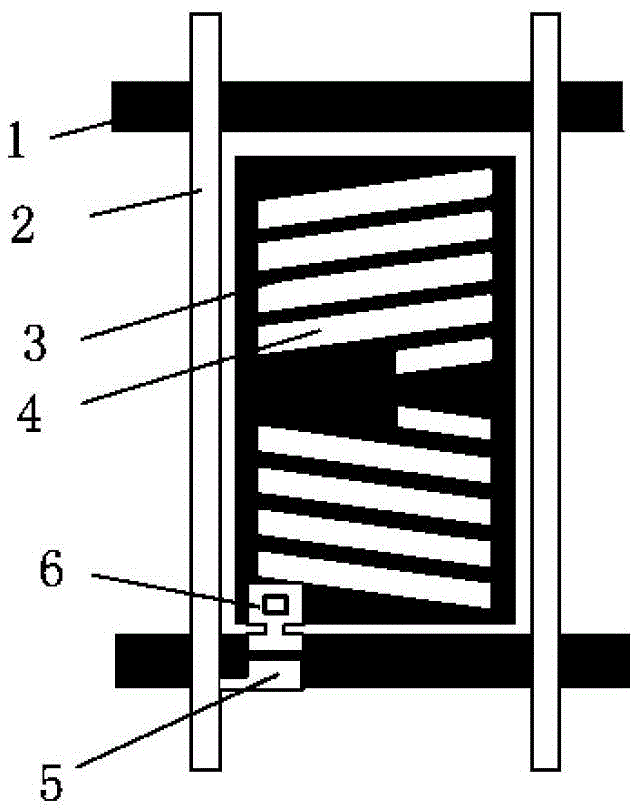
[0048] The array substrate of this embodiment is such as Figure 7 As shown, the structure of the array substrate in Embodiment 1 is basically the same. The difference is that in this embodiment, two independent thin film transistors (one gate, one source, and one drain) are used instead of the composite thin film transistor with common source and double drain. The gates of the two thin film transistors are located on the gate line 1 or connected to the gate line 1, the source electrodes 5 are connected to the data line 2, and the drain electrodes 6 are connected to the pixel electrodes 3 in the two display areas respectively, and the respective electrodes of the two thin film transistors The source-drain channels formed between the source 5 and the drain 6 have different channel widths.

[0049] Wherein, the channel widths of the respective source and drain channels of the two thin film transistors range from 20 to 30 um.

[0050] The rest of the structure is the same as th...

Embodiment 3

[0056] This embodiment also provides a display device, including the array substrate in any one of the above embodiments. The display device may be any product or component with a display function such as a liquid crystal panel, a liquid crystal TV, a liquid crystal display, a digital photo frame, a mobile phone, and a tablet computer.


PUM


Abstract

The invention discloses an array substrate and relates to the technical field of displaying. The array substrate comprises a substrate, grid lines, data lines and pixel units, wherein the grid lines and the data lines are formed on the substrate; each pixel unit is driven by the same grid line and the same data line, and comprises a thin film transistor structure and at least two display regions; and the thin film transistor structure drives pixel electrodes in the at least two display regions simultaneously to enable voltages applied to the pixel electrodes in the at least two display regions to be different. The invention further discloses a display device comprising the array substrate. In the array substrate, each pixel unit is divided into at least two independent display regions and different voltages are applied to the pixel electrodes in the at least two regions, so that liquid crystal molecules in each pixel unit have at least two deflection angles, the luminance difference of a liquid crystal display is reduced and the color difference is further reduced.

Description

technical field [0001] The present invention relates to the field of display technology, in particular to an array substrate and a display device. Background technique [0002] Advanced Super Dimension Switch (AD-SDS, ADS for short) mode liquid crystal display has the advantages of wide viewing angle, high transmittance, low chromatic aberration, etc., and has gradually been widely used. Specifically, the ADS technology mainly uses the electric field generated by the edge of the slit electrode in the same plane and the electric field generated between the slit electrode layer and the plate electrode layer to form a multi-dimensional electric field, so that everything between the slit electrodes and directly above the electrodes in the liquid crystal cell All aligned liquid crystal molecules can be rotated, thereby improving the working efficiency of the liquid crystal and increasing the light transmission efficiency. Advanced ultra-dimensional field conversion technology ca...

Claims


Application Information

Patent Timeline
Patent Type & Authority Applications(China)
IPC IPC(8): G02F1/1362G02F1/1368G02F1/1343H01L27/12
CPCG02F2001/134345G02F1/134309G02F1/13624G02F1/133707G02F1/1368G02F1/134345
Inventor 张新霞涂志中郭霄吕凤珍林炳仟
Owner BOE TECH GRP CO LTD
Why Eureka
Try Eureka