Method, device and system for detecting printed circuit board (PCB)

A technology of PCB board and detection method, applied in the field of PCB board detection, can solve the problems that PCB board detection is susceptible to external interference, strong subjectivity, and high missed detection rate, and achieves low false detection rate, low resolution efficiency, and high detection efficiency. Effect

Active Publication Date: 2013-02-20
STATE GRID ZHEJIANG ELECTRIC POWER CO MARKETING SERVICE CENT +1
View PDF11 Cites 50 Cited by
  • Summary
  • Abstract
  • Description
  • Claims
  • Application Information

AI Technical Summary

Problems solved by technology

[0005] In view of this, the present invention provides a PCB board detection method, device and system to solve the problems of low efficiency, high missed detecti...

Method used


Image

  • Method, device and system for detecting printed circuit board (PCB)
  • Method, device and system for detecting printed circuit board (PCB)
  • Method, device and system for detecting printed circuit board (PCB)

Examples


Embodiment 1

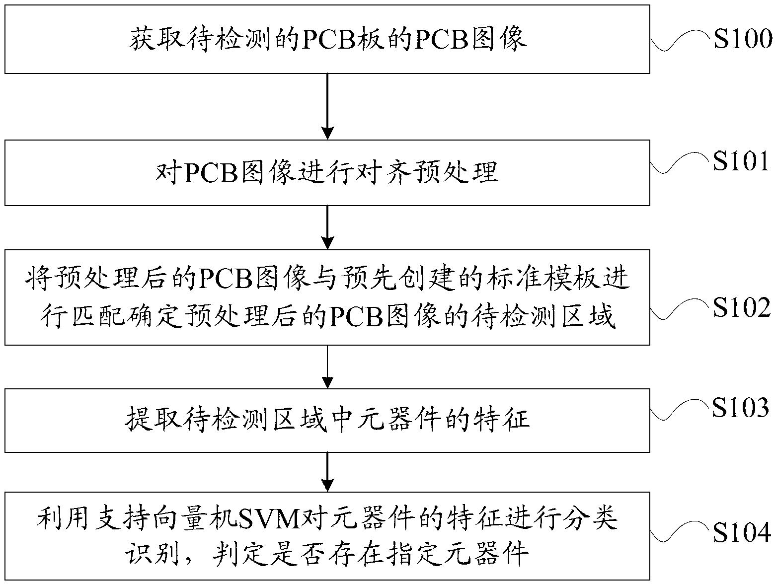
[0048] Embodiment 1 of the present invention provides a PCB detection method, figure 1 It is a schematic flow chart of the method, and the method includes:

[0049] S100: Acquire a PCB image of the PCB board to be detected.

[0050] S101: Perform alignment preprocessing on the acquired PCB image.

[0051] S102: Match the preprocessed PCB image with a pre-created standard template, and determine a region to be detected in the preprocessed PCB image when a matching condition is met.

[0052] S103: Extract features of components in the area to be detected.

[0053] S104: Use the pre-trained support vector machine (SVM) to classify and identify the features of the components, and determine whether the specified components exist in the area to be detected based on the classification and identification results.

[0054] The PCB board detection method provided by Embodiment 1 of the present invention can locate the detection area and determine whether there are specified component...

Embodiment 2

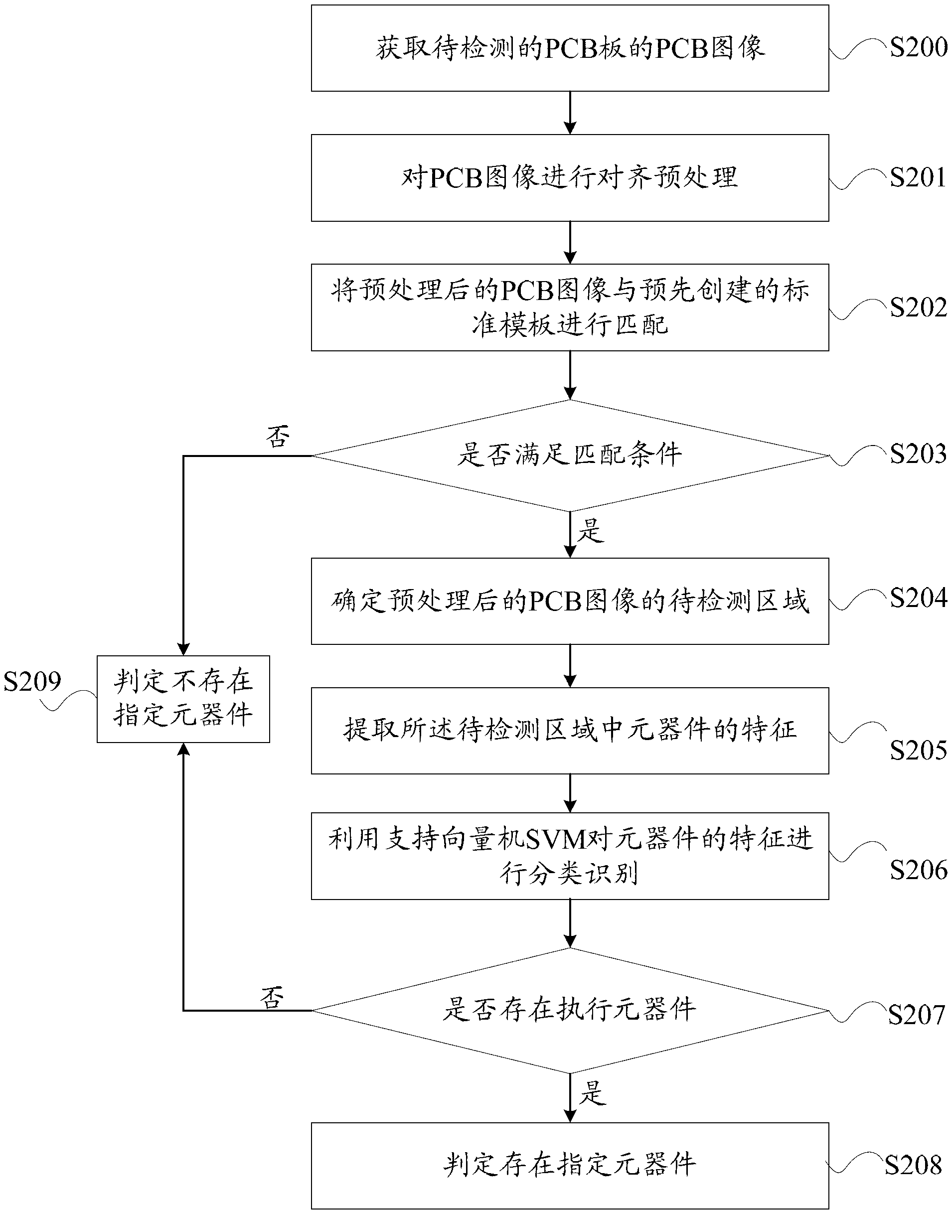
[0056] The embodiment of the present invention provides a PCB board detection method, figure 2 It is a schematic flow chart of the method, and the method may include:

[0057] S200: Acquire a PCB image of the PCB board to be detected.

[0058] S201: Perform alignment preprocessing on the PCB image.

[0059] When shooting the PCB image of the PCB board, due to various reasons, the captured PCB board will have a certain inclination on the image, and sometimes the inclination angle may be larger, and the image alignment preprocessing is to make the edge of the PCB board as close as possible Vertical state or horizontal state, which is consistent with the sampling state of the standard template.

[0060] In this embodiment, step S201 may include:

[0061] S201a: Using the background difference method to obtain the PCB board object by using the PCB image and the pre-constructed background image.

[0062] Among them, the background image can be constructed in the following manner...

Embodiment 3

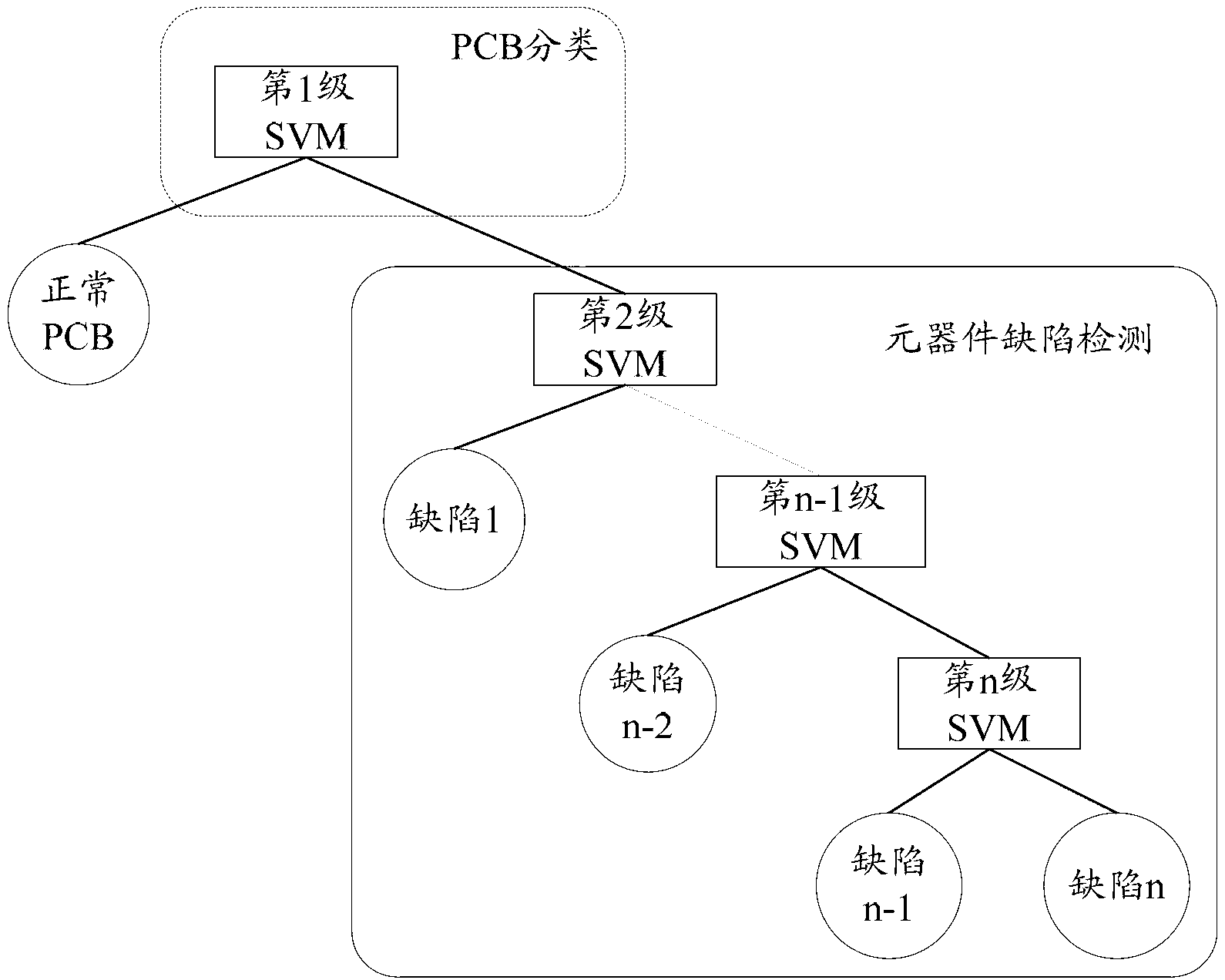
[0122] Embodiment 3 of the present invention provides a PCB board detection device, Figure 4 It is a schematic structural diagram of the device, which includes: an acquisition unit 100 , a preprocessing unit 101 , a matching unit 102 , a determination unit 103 , an extraction unit 104 , a classification unit 105 and a determination unit 106 . in:

[0123] The obtaining unit 100 is configured to obtain a PCB image of the PCB board to be detected. The preprocessing unit 101 is configured to perform alignment preprocessing on the PCB image acquired by the acquiring unit 100 . The matching unit 102 is configured to match the PCB image preprocessed by the preprocessing unit 101 with the pre-created standard template. The determination unit 103 is configured to determine the area to be detected in the preprocessed PCB image when the matching condition is satisfied. The extraction unit 104 is configured to extract features of components in the area to be detected determined by th...


PUM


Abstract

The invention provides a method, device and system for detecting a printed circuit board (PCB). The method includes: obtaining a PCB image of a PCB to be detected, conducting alignment pre-processing on the PCB image, and matching the pre-processed PCB image with a standard form built in advance. When matching conditions are met, an area to be detected of the pre-processed PCB image is determined, and features of components in the area to be detected are extracted. A support vector machine (SVM) is used for identifying the features of the components, and whether appointed components exist in the area to be detected is judged through a distinguishing result. The method, device and system is simple to achieve, high in detection efficiency and low in false detecting rate and solves the problem in a traditional manual detection method of being low in efficiency, high in omission rate, strong in subjectivity and easy to be subject to external disturbance during detection of a PCB.

Description

technical field [0001] The invention relates to the technical field of PCB board detection, in particular to a PCB board detection method, device and system. Background technique [0002] Smart energy meter is a new type of all-electronic energy meter, which has the functions of electric energy measurement, real-time monitoring, automatic control, information interaction and data interaction, etc. It is convenient for users to accurately and quickly understand the electricity consumption of the family and formulate energy-saving plans. [0003] Printed Circuit Board (PCB) is the core component of the smart energy meter, and it is the matrix that carries various electronic components. Each smart energy meter has a PCB and a large number of components, such as resistors, capacitors, and inductors. , integrated chips, etc., these components are mainly welded on the PCB board with surface mount technology (Surface Mount Technology, SMT) and socket mounting technology. [0004] ...

Claims


Application Information

Patent Timeline
IPC IPC(8): G01N21/88
Inventor 李少腾姚力胡瑛俊楼轶吴幸
Owner STATE GRID ZHEJIANG ELECTRIC POWER CO MARKETING SERVICE CENT
Why Eureka
Try Eureka