Array substrate manufacturing method, array substrate and display device

A technology of an array substrate and a manufacturing method, which is applied in the display field, can solve the problems affecting the product yield rate and data line disconnection defects, and achieves the effect of reducing the probability of disconnection defects and improving the yield rate.

Inactive Publication Date: 2015-02-04
BOE TECH GRP CO LTD
View PDF4 Cites 0 Cited by
  • Summary
  • Abstract
  • Description
  • Claims
  • Application Information

AI Technical Summary

Problems solved by technology

[0003] When the display resolution is increased to 300ppi or even 400ppi, 500ppi and above, it is necessary to reduce the line width of the data line from above 4um to 2-3um (products with a resolution above 300ppi are called high-resolution products with narrow line width) or narrow line width products), and at present, the wet etching process is generally used to prepare the data lines and source and drain electrodes, but when the line width of the data lines is reduced to 2-3um, due to the uniformity of wet etching, the data The wire is prone to broken wires, which seriously affects the yield of the product

Method used


Image

  • Array substrate manufacturing method, array substrate and display device
  • Array substrate manufacturing method, array substrate and display device
  • Array substrate manufacturing method, array substrate and display device

Examples


Embodiment 1

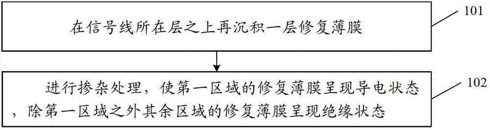
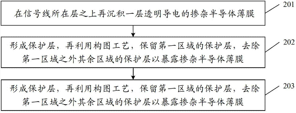
[0050] An embodiment of the present invention provides a method for manufacturing an array substrate. The array substrate includes: a display unit and signal lines for providing display signals and control signals to the display unit, such as figure 1 As shown, the method includes:

[0051] 101. Form a repair film on the layer where the signal line is located, and the repair film is a transparent conductive doped semiconductor film or a transparent insulating semiconductor film;

[0052] The signal lines in this step may be data lines, or gate lines, or common electrode lines, or two of them are in the same layer.

[0053] In this step, after the signal line is formed, a repair film layer is formed. The repair film layer can be a transparent conductive doped semiconductor film, such as an amorphous silicon (a-si) material doped with boron B or phosphorus P, or Tin-doped indium oxide (Indium Tin Oxides, ITO), or N-type or P-type doped thin films of materials such as ZnO, ZnS, ...

Embodiment 2

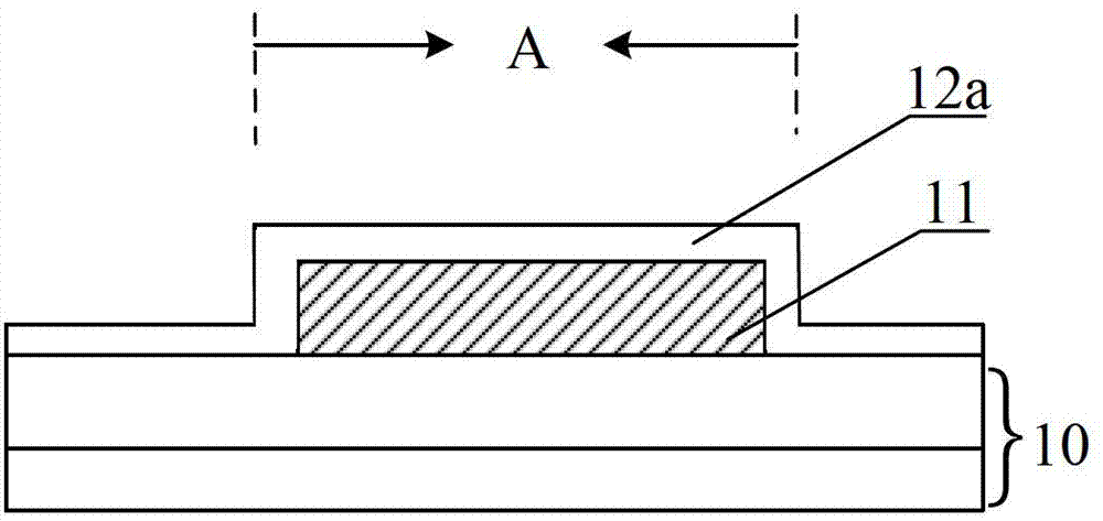
[0086] Such as Figure 6 and Figure 7 As shown, the embodiment of the present invention also provides an array substrate, including: a display unit 15 and a signal line that provides display signals and control signals to the display unit 15, and the signal line can be a data line, or a gate line, or a common electrode line , for example, the signal line is the data line 112 in the figure,

[0087] A repair film 12 is arranged on the layer where the signal line (data line 112) 11 is located, and,

[0088] The repair film 12 is in a conductive state in the first region A, and is in an insulating state in other regions except the first region A, where the first region A is the region corresponding to the signal line 11 .

[0089] In this embodiment, the repair film 12 acts as a passivation layer at the same time, the repair film 12 above the data line (the first region A) is in a conductive state, and the rest of the region (except the first region A) the repair film 12 is in...


PUM


Abstract

The invention discloses an array substrate manufacturing method, an array substrate and a display device and relates to the field of displaying, and the method is used for reducing the probability of breakage of signal wires and improving the product yield and is especially suitable for a high-resolution product with a narrow line width. The array substrate manufacturing method comprises the following steps of: forming a layer of repairing thin film on a layer in which the signal wire is positioned, wherein the repairing thin film is a transparent conductive doped semiconductor thin film or a transparent insulative semiconductor thin film; and performing conversion processing, wherein the repairing thin film in the first region is in a conductive state, the repairing thin film in other regions except for the first region is in an insulative state, and the first region is a region in which the signal wire is positioned. The array substrate comprises a display unit and the signal wire, wherein the repairing thin film is arranged on the layer in which the signal wire is positioned; and the repairing thin film is in the conductive state in the first region and is in the insulation state in other regions except for the first region.

Description

technical field [0001] The present invention relates to the field of display technology, in particular to a method for manufacturing an array substrate, an array substrate, and a display device. Background technique [0002] With people's continuous pursuit of display quality, high resolution has become a major trend in the development of displays. However, as the resolution of the display increases, the line width of the data line wiring also needs to be reduced accordingly, which puts forward higher requirements on the manufacturing process. [0003] When the display resolution is increased to 300ppi or even 400ppi, 500ppi and above, it is necessary to reduce the line width of the data line from above 4um to 2-3um (products with a resolution above 300ppi are called high-resolution products with narrow line width) or narrow line width products), and at present, the wet etching process is generally used to prepare the data lines and source and drain electrodes, but when the...

Claims


Application Information

Patent Timeline
Patent Type & Authority Patents(China)
IPC IPC(8): H01L21/48H01L23/50
Inventor 曹占锋戴天明姚琪
Owner BOE TECH GRP CO LTD
Why Eureka
Try Eureka