Processing method of printed wiring board with ultra-small solder mask intervals

A technology for printed circuit boards and processing methods, which is applied to the secondary treatment of printed circuits and the application of non-metallic protective layers. It can solve problems such as wire separation, achieve easy control, prevent falling off, and improve product quality.

Inactive Publication Date: 2013-02-20
DALIAN PACIFIC ELECTRONICS
View PDF3 Cites 3 Cited by
  • Summary
  • Abstract
  • Description
  • Claims
  • Application Information

AI Technical Summary

Problems solved by technology

[0003] In order to overcome the deficiencies in the above-mentioned prior art, the object of the present invention is to provide a processing method for printed circuit boards with ultra-small solder mask spacing, which solves the problem of line drop-off that cannot be solved by traditional screen printing technology

Method used


Image

  • Processing method of printed wiring board with ultra-small solder mask intervals
  • Processing method of printed wiring board with ultra-small solder mask intervals
  • Processing method of printed wiring board with ultra-small solder mask intervals

Examples


Embodiment Construction

[0019] The present invention will be further described below in conjunction with accompanying drawing.

[0020] First, surface activation treatment is carried out on the printed circuit board, and screen printing of the solder resist ink is carried out within 4 hours after the treatment; after the screen printing of the solder resist ink, it is exposed→developed→cured deal with.

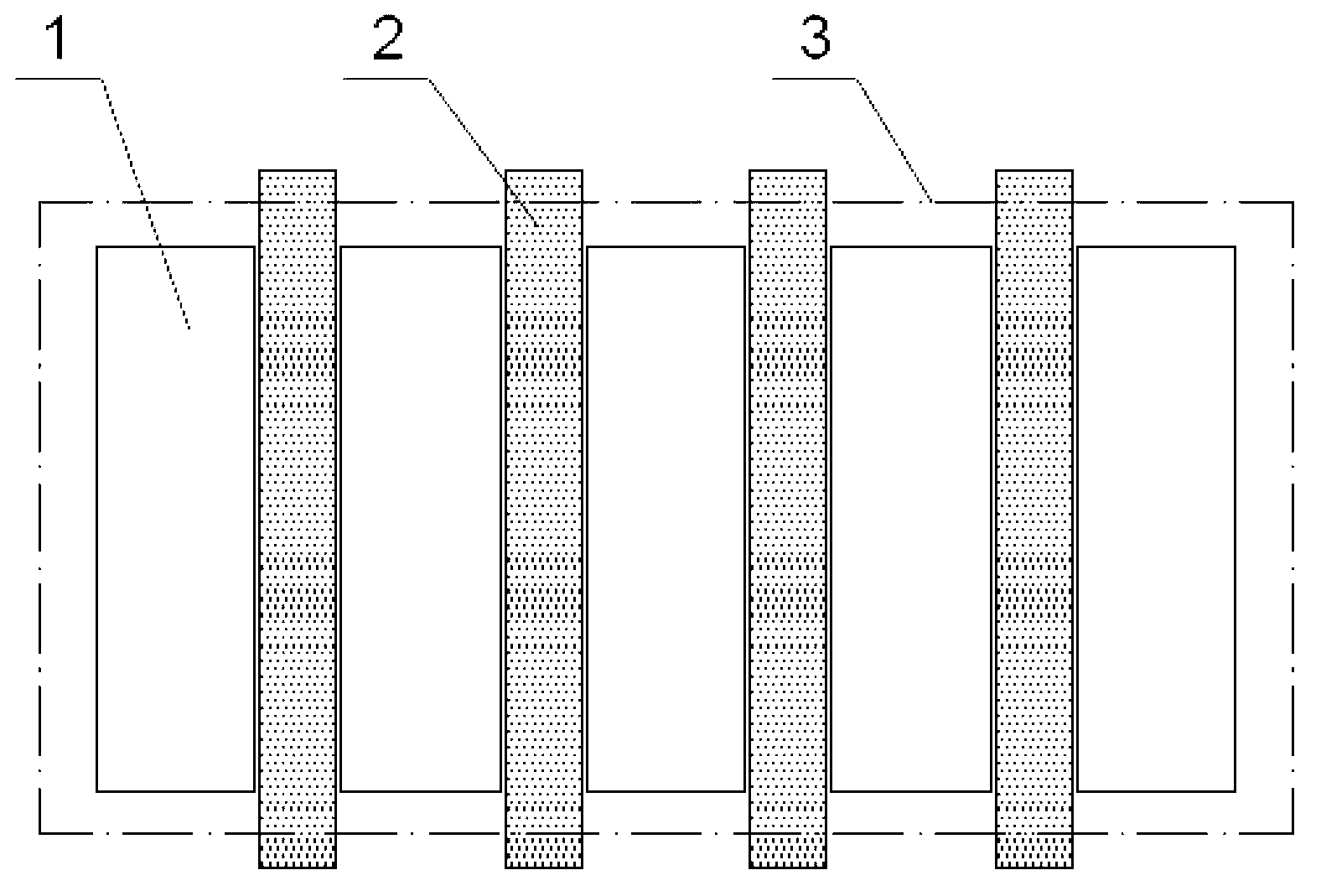
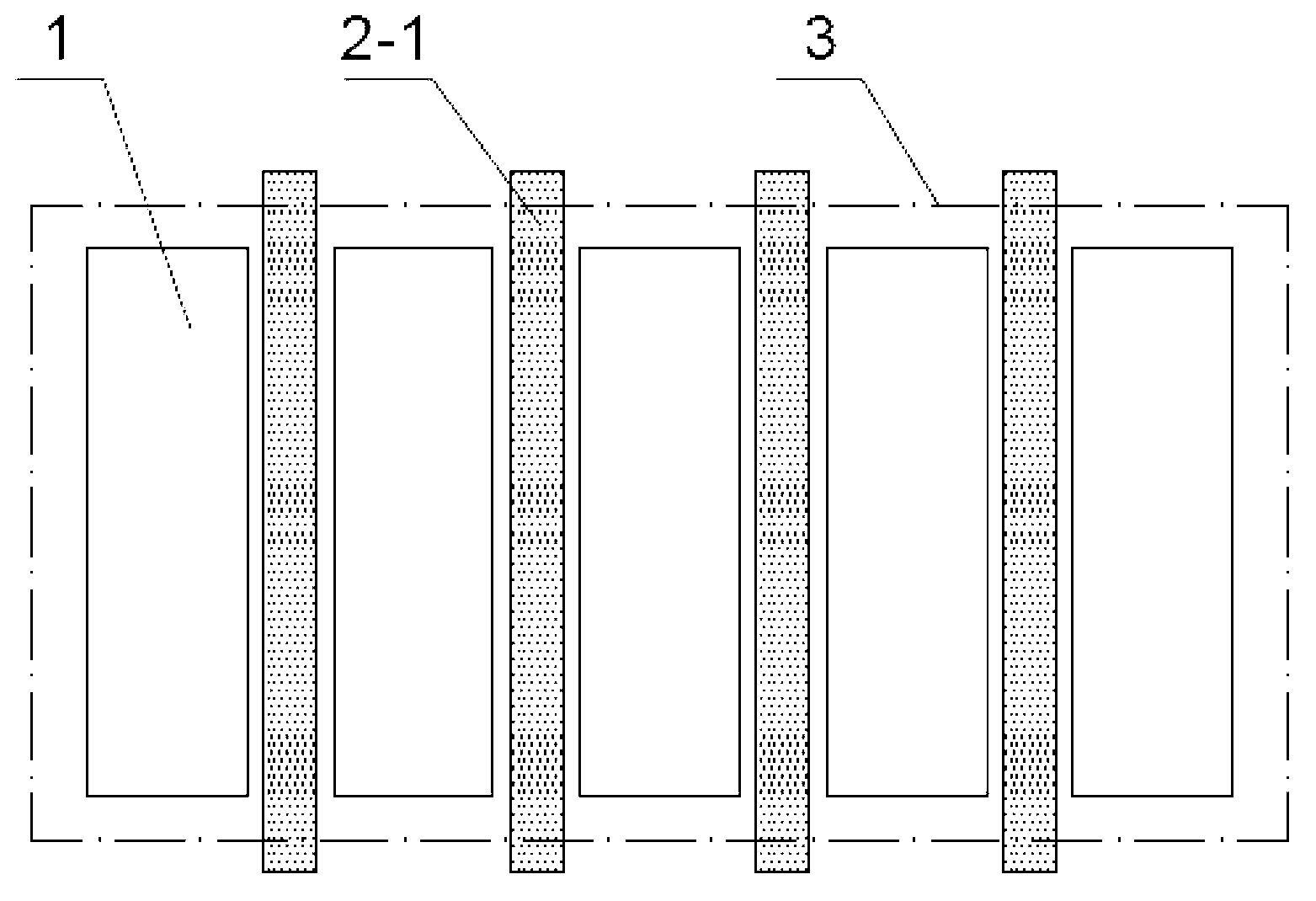
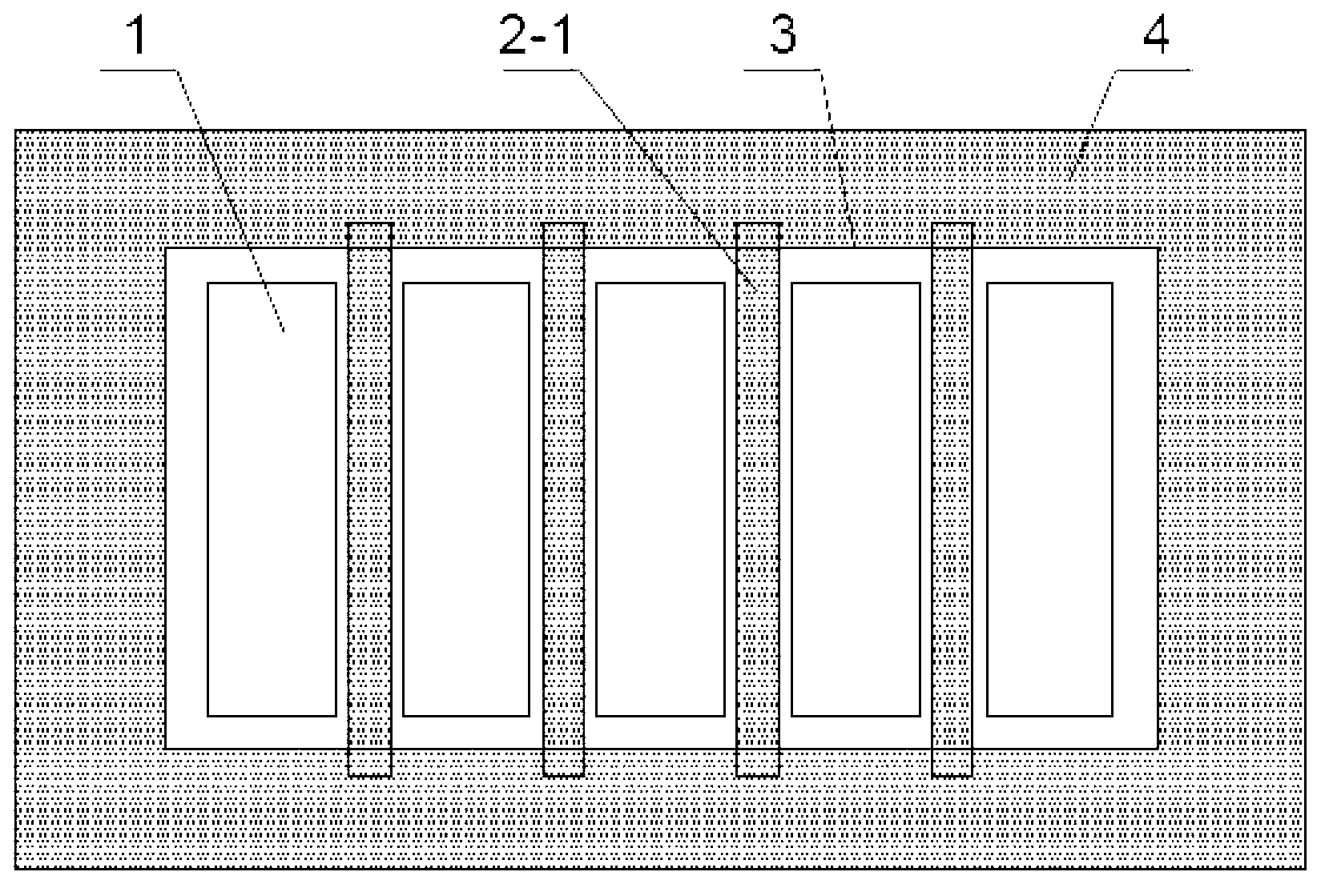
[0021] Such as figure 1 As shown, the screen printing ink 2 is printed between the SMD pads 1, the thickness of the solder resist ink of the screen printing is half the ink thickness according to the customer's requirement, and the spacer 2-1 Both ends of the printing length exceed the annual ring of the SMD pad space by 1-1.5mil. When exposing, the film used is only designed to expose the exposure area at the line 2-1, and the other areas are black areas without exposure, and the annual ring of the empty area of ​​the SMD pad 1 at the line 2-1 is designed to be 1mil. The curing temperature is con...


PUM


Abstract

The invention relates to a processing method of a printed wiring board and relates to a processing method of a printed wiring board with ultra-small solder mask intervals. The method includes the following steps of firstly, subjecting the printed wiring board to surface activating treatment, and then subjecting solder resist ink separation lines of the printed wiring board to screen printing in four hours after treatment; subjecting the printed wiring board to exposing, developing and solidifying at the temperature of 150 DEG C for 30 minutes after the screen printing of the solder resist ink separation lines; subjecting the solidified printed wiring board to surface activating treatment and then subjecting the solder resist ink separation lines of of the whole printed wiring board to electrostatic spraying in four hours after treatment; subjecting the printed wiring board to preliminary drying at the temperature of 80 DEG C for 40-50 minutes; and subjecting the preliminarily dried printed wiring board to exposing, developing and solidifying at the temperature of 150 DEG C for 60 minutes. By means of the processing method, the problem of poor binding forces between separation line ink and a printed wiring board base material is solved, and dropping of the solder resist ink separation lines is prevented in the process of subsequent processing.

Description

technical field [0001] The invention relates to a processing method of a printed circuit board, and more specifically, relates to a processing method of a printed circuit board with an ultra-small solder-proof spacing. Background technique [0002] With the development of electronic information technology, electronic products are developing in the direction of light weight, miniaturization, and high speed, which puts forward higher requirements for printed boards. In the era of high-density connection (HDI) technology, line width and line spacing will be There is an inevitable trend towards smaller and denser. In order to adapt to this development trend, printed circuit board designers and manufacturers are constantly updating design concepts and manufacturing methods. As the design density of printed circuit boards increases, the accuracy requirements for the solder resist ink layer are also increasing. For printed circuit boards that require ultra-small solder mask spaci...

Claims


Application Information

Patent Timeline
Patent Type & Authority Applications(China)
IPC IPC(8): H05K3/28
Inventor 牛凯崔连旺陈志强
Owner DALIAN PACIFIC ELECTRONICS
Why Eureka
Try Eureka