
Mask plate and manufacturing method thereof

A technology of mask plate and light-transmitting film, which is applied in the field of mask plate and its preparation, can solve problems such as many burrs, difficult control of line width, and insufficient smoothness, so as to achieve good diffraction effect and improve control accuracy

Active Publication Date: 2015-01-07
HEFEI BOE OPTOELECTRONICS TECH +1
View PDF6 Cites 0 Cited by
  • Summary
  • Abstract
  • Description
  • Claims
  • Application Information

AI Technical Summary

Problems solved by technology

The advantage of using this mask to prepare narrow line widths is that the effect of narrow line width can be achieved only by changing the sawtooth design of the non-transparent area in the mask. However, the burrs on both sides of the structure obtained by using this mask are relatively small. much, not smooth enough
[0006] SSM (Slit Shot mask) mask design, such as figure 2 as shown, figure 2 The mask plate shown adjusts the exposure amount by reducing the width a of its non-transparent region 02, and then obtains a photoresist with a narrower line width. This method just utilizes the diffraction of light, but after exposure and development, the substrate It is difficult to control the line width of the remaining photoresist 021 on 04, and it is difficult to control the line width of the final structure
[0007] GTM mask design such as image 3 as shown, image 3 The mask shown in the mask changes the transmittance of each part of the non-transparent region through the stepped non-transparent region. For example, the transmittance of the middle part 032 of the non-transparent region is smaller than the transmittance of the edge part 031. In order to achieve the effect of narrow line width, image 3 In the non-transmissive area shown in , the light transmittance is shown by the broken line 034; although this mask can also obtain photoresist 033 with a narrow line width, when using this mask for exposure, its non-transmissive The diffraction effect of light at the edge of the light area is also difficult to control, and the obtained line width is also difficult to control

Method used


Image

  • Mask plate and manufacturing method thereof
  • Mask plate and manufacturing method thereof
  • Mask plate and manufacturing method thereof

Examples


Embodiment Construction

[0038] The following will clearly and completely describe the technical solutions in the embodiments of the present invention with reference to the accompanying drawings in the embodiments of the present invention. Obviously, the described embodiments are only some, not all, embodiments of the present invention. Based on the embodiments of the present invention, all other embodiments obtained by persons of ordinary skill in the art without making creative efforts belong to the protection scope of the present invention.

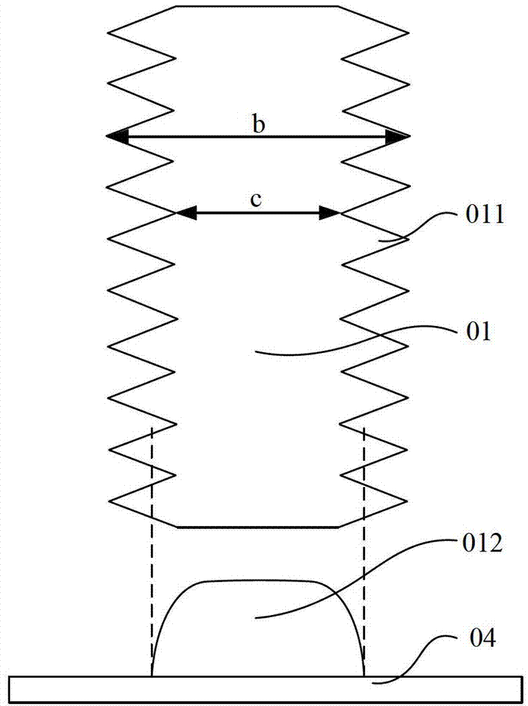
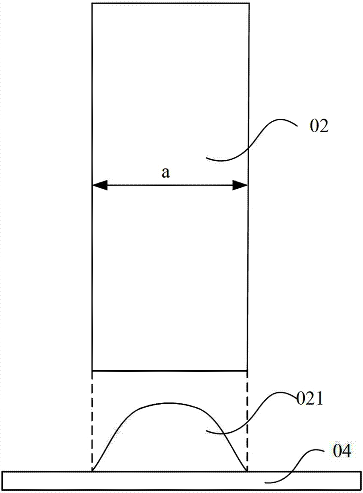
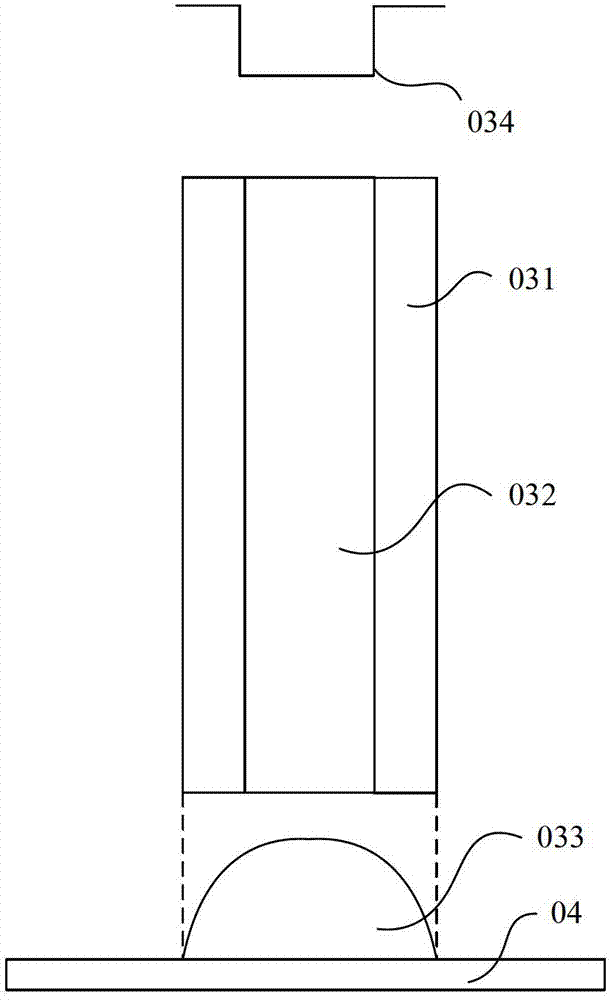
[0039] Such as Figure 4 As shown, the mask plate provided by the present invention includes a mask plate body 1, the mask plate body 1 has a non-transparent area 12 and a light-transmitting area 11, and the light-transmitting area 11 has a light-transmitting area made of photoresist. film 111 , the light absorbance of the light-transmitting film 111 gradually increases from the center line to the non-light-transmitting regions on both sides.

[0040] Please ...


PUM


Abstract

Embodiments of the present invention disclose a mask plate and a manufacturing method thereof. The mask plate includes a mask plate body and a transmissive member, wherein the mask plate body has a transmissive part and a non-transmissive part adjacent to the transmissive part, the transmissive member is disposed corresponding to the transmissive part of the mask plate body, the absorbance of the transmissive member progressively increases in a direction away from a center region of the transmissive member to a edges region of the transmissive member close to the non-transmissive part.

Description

technical field [0001] The invention relates to the technical field of display panel processing, in particular to a mask plate and a preparation method thereof. Background technique [0002] In the field of display panel technology, with the development of high-resolution display technology, the number of pixels per unit size in the display panel is gradually increasing, and the pixel size is continuously decreasing. In order to maintain the aperture ratio, the pixel array in the array substrate The line width of the electrode wiring and the black matrix in the color filter substrate should also be reduced accordingly. [0003] In the preparation process of narrow line width, the essence of light is electromagnetic wave, and the diffraction effect of electromagnetic wave itself, in the traditional exposure and development process, it is difficult to realize the narrow line width process. [0004] In order to overcome the influence of the above-mentioned light diffraction ef...

Claims


Application Information

Patent Timeline
Patent Type & Authority Patents(China)
IPC IPC(8): G03F1/54
CPCG03F1/38G03F1/56
Inventor 徐向阳邓立赟金玟秀杜雷王凯张敏
Owner HEFEI BOE OPTOELECTRONICS TECH
Features
  • Generate Ideas
  • Intellectual Property
  • Life Sciences
  • Materials
  • Tech Scout
  • Unparalleled Data Quality
  • Higher Quality Content
  • 60% Fewer Hallucinations
Learn More