A finfet and an application circuit using the finfet

An N-type, voltage technology, applied in the direction of circuits, electrical components, electronic switches, etc., to achieve the effect of reducing leakage current and reducing switching power loss

Active Publication Date: 2015-12-09
WUXI ZGMICRO ELECTRONICS CO LTD
View PDF6 Cites 0 Cited by
  • Summary
  • Abstract
  • Description
  • Claims
  • Application Information

AI Technical Summary

Problems solved by technology

In the traditional field effect transistor structure, the gate that controls the passage of current can only control the on and off of the circuit on one side of the gate, which belongs to the planar structure.

Method used


Image

  • A finfet and an application circuit using the finfet
  • A finfet and an application circuit using the finfet
  • A finfet and an application circuit using the finfet

Examples


Embodiment Construction

[0021] In order to make the above objects, features and advantages of the present invention more comprehensible, the present invention will be further described in detail below in conjunction with the accompanying drawings and specific embodiments.

[0022] Reference herein to "one embodiment" or "an embodiment" refers to a particular feature, structure or characteristic that can be included in at least one implementation of the present invention. "In one embodiment" appearing in different places in this specification does not all refer to the same embodiment, nor is it a separate or selective embodiment that is mutually exclusive with other embodiments. Unless otherwise specified, the words connected, connected, and joined in this document mean that they are electrically connected directly or indirectly.

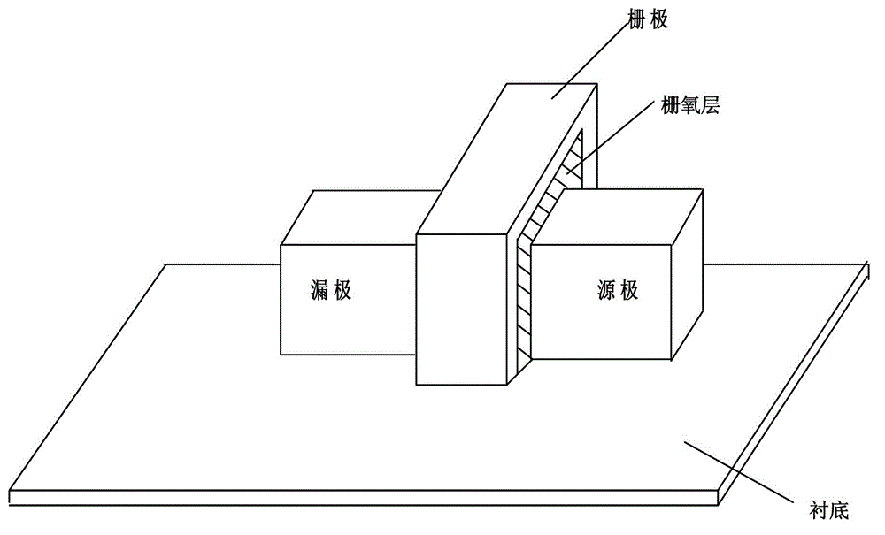
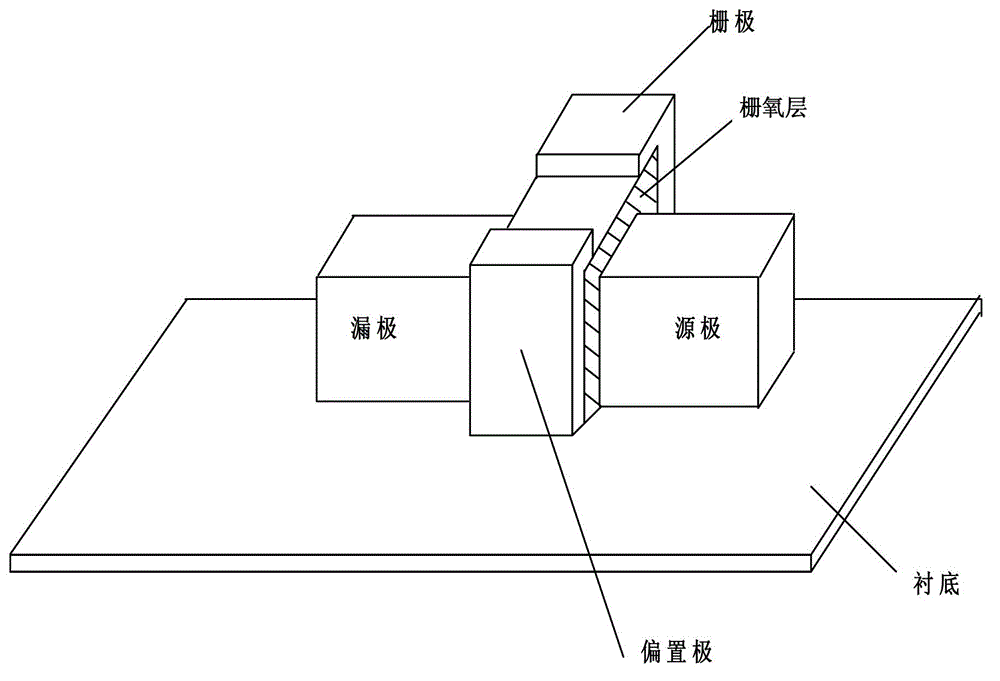
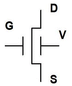
[0023] In the FINFET of the present invention, the gate in the prior art is divided into a gate and a bias electrode, and the bias electrode is connected to a bias voltage,...


PUM


Abstract

The invention provides an FINFET (Fin-Field-Effect-Transistor) and an application circuit applying the FINFET. The FINFET comprises a source electrode, a gate electrode, a drain electrode and a bias electrode, wherein the source electrode and the drain electrode are formed on a substrate, a channel area is formed between the source electrode and the drain electrode, a gate-oxide layer is formed at the outer side of the channel area, the gate electrode and the bias electrode are formed at the outer side of the gate-oxide layer, and a certain distance is formed between the gate electrode and the bias electrode. Compared with the prior art, the FINFET disclosed by the invention has the advantages that the gate electrode in the prior art is divided into the gate electrode and the polarization electrode, and the bias electrode is connected to offset voltage, so that the leakage between the drain electrode and the source electrode can be reduced when the FINFET is switched off, and meanwhile, the power consumption on the switching on and off of the FINFET can be reduced.

Description

【Technical field】 [0001] The invention relates to the field of semiconductors, in particular to a FINFET and an application circuit using the FINFET. 【Background technique】 [0002] With the continuous evolution of integrated circuit technology, the channel length of field effect transistors (Field Effect Transistor, FET) is continuously reduced. The continuous reduction of the channel length can realize the continuous reduction of the device area, so that more wafers can be produced on the wafer with the same area, thereby reducing the cost of the wafer. The characteristic size of a general process is the minimum channel length. For example, the 28nm process means that the minimum channel length of its field effect transistor is 28nm. When the process evolves below 28nm, the planar process becomes more and more difficult to manufacture. The reason is that when the channel length is too small, the leakage between the drain and source of the device becomes larger and larger,...

Claims


Application Information

Patent Timeline
Patent Type & Authority Patents(China)
IPC IPC(8): H01L29/423H01L29/78H03K17/687
CPCH01L29/7855
Inventor 王钊
Owner WUXI ZGMICRO ELECTRONICS CO LTD
Why Eureka
Try Eureka