Switching power supply capable of avoiding coupling effect

A switching power supply and coupling effect technology, applied in electronic switches, circuits, electrical components, etc., can solve problems such as switching power loss, reduce switching power loss, avoid coupling effect, and improve power efficiency.

Inactive Publication Date: 2013-12-04
NVIDIA CORP
View PDF2 Cites 0 Cited by
  • Summary
  • Abstract
  • Description
  • Claims
  • Application Information

AI Technical Summary

Problems solved by technology

and figure 1 Similar to a switching power supply in buck mode, the figure 2 In the boost mode switching power supply 200 shown, there is also a coupling effect in the area where the parasitic inductance 202 near the source of the power MOSFET 205 is located, and this coupling effect also causes a large switching power loss

Method used


Image

  • Switching power supply capable of avoiding coupling effect
  • Switching power supply capable of avoiding coupling effect
  • Switching power supply capable of avoiding coupling effect

Examples


Embodiment Construction

[0034] In this application, exemplary embodiments will be described around a switching power supply avoiding coupling effects. Those of ordinary skill in the art should realize that the following description is only exemplary and not intended to be limiting in any way. Inspiration for other embodiments will readily occur to those skilled in the art having the benefit of this application. Now, implementation of the exemplary embodiments as shown in the accompanying drawings will be described in more detail. Wherever possible, the same reference numbers will be used throughout the drawings and the following description to refer to the same or like items.

[0035] Reference will now be made in detail to the preferred embodiments of the invention, examples of which are illustrated in the accompanying drawings.

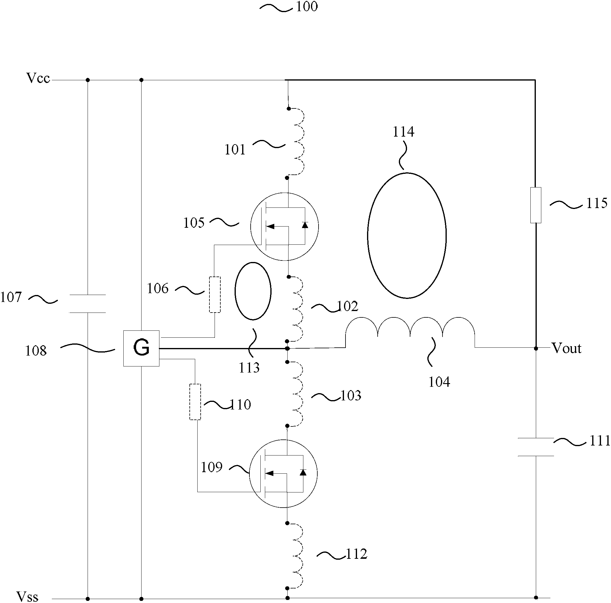
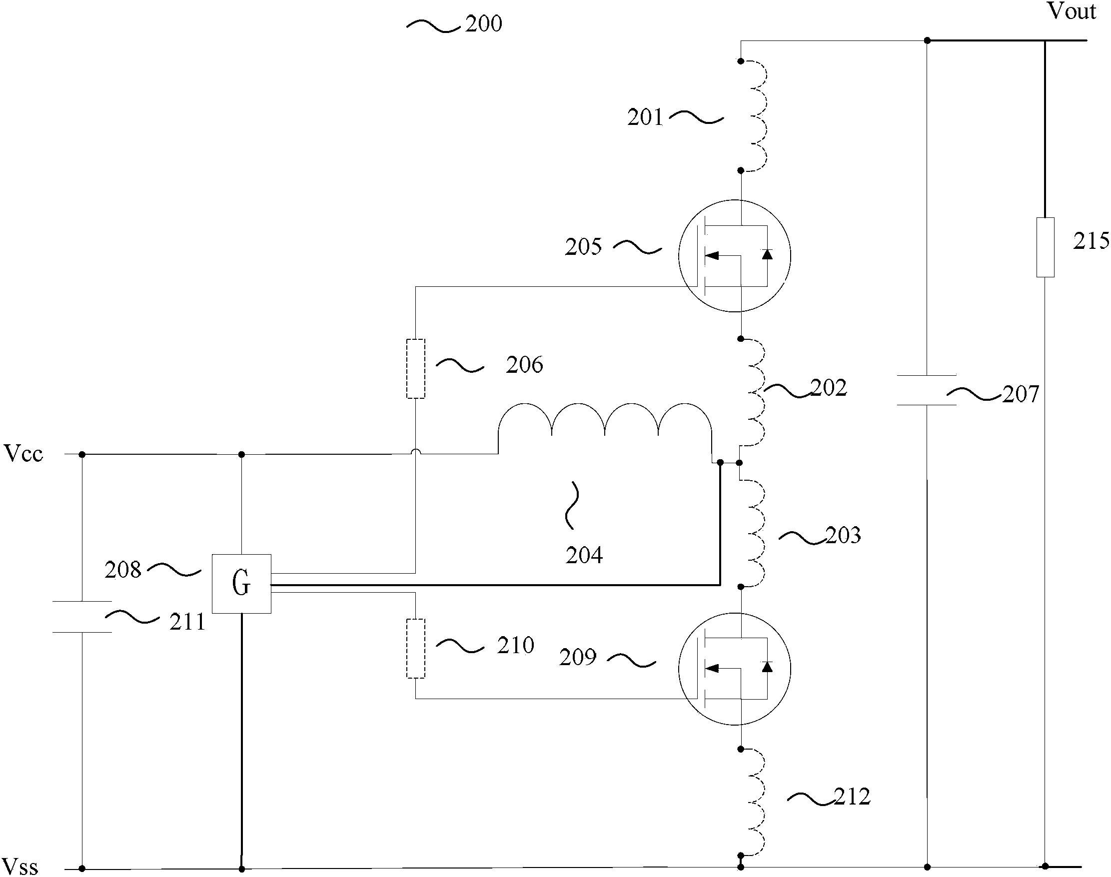
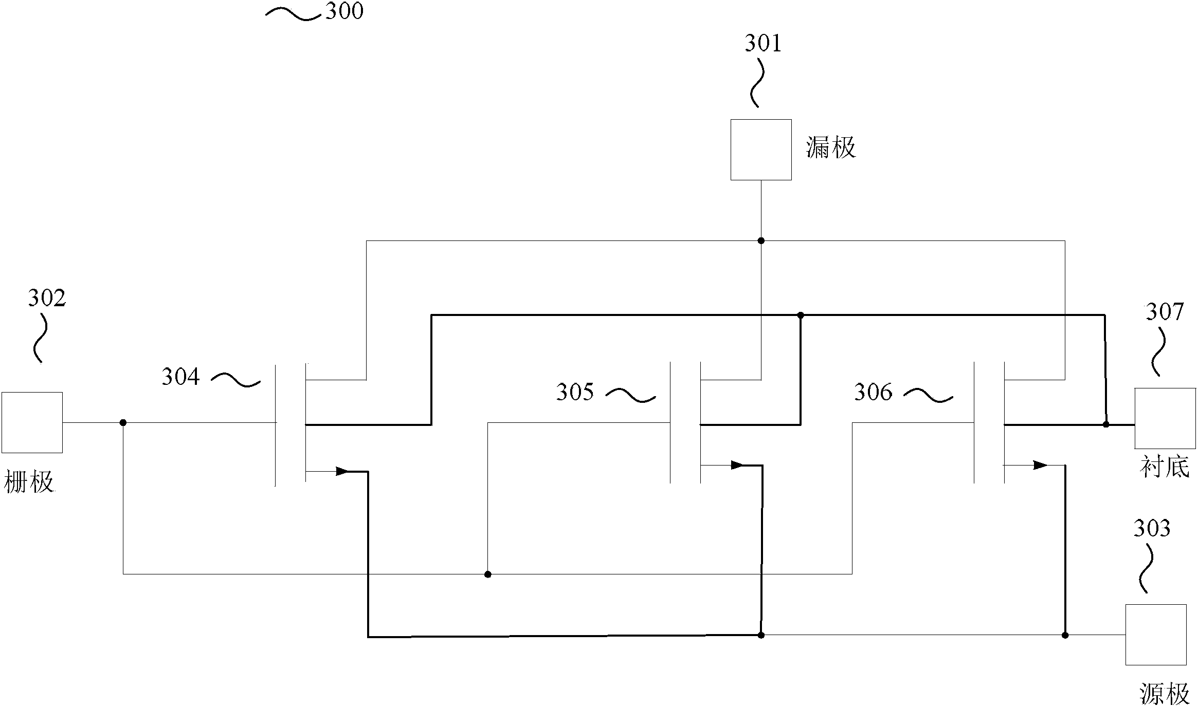
[0036] To solve the problem of power loss caused by the internal coupling effect of the switching power supply in the prior art, the present invention improves the struc...


PUM


Abstract

A switching power capable of avoiding coupling effects is provided. The switching power comprises a driving loop. The driving loop comprises the substrate end and the gate end of a power Metal-Oxide-Semiconductor Field-Effect Transistor (MOSFET) and a controlling gate, and the controlling gate is connected to the gate end of the power MOSFET and the substrate end of the power MOSFET is connected to the controlling gate. The switching power provided by the present can avoid the coupling effect of the driving loop and the power stage loop at the common source pin, thereby reducing the switching power losses and improving the efficiency of the switching power.

Description

technical field [0001] The invention relates to a switching power supply, in particular to a switching power supply capable of avoiding coupling effects. Background technique [0002] In the switching power supply of the prior art, the power Metal-Oxide-Semiconductor Field-Effect Transistor (MOSFET) is a field-effect transistor (field-effect transistor) that can be widely used in the switching power supply. . The switching power supply includes a drive circuit and a power circuit, wherein the drive circuit drives the input capacitance of the power MOSFET to charge or discharge, so that the power MOSFET is turned on or off, and the power circuit is the main path for generating large loading current. The drive circuit and the power circuit have a common pin at the source, which causes a coupling effect between the drive circuit and the power circuit, especially when a large current is loaded, and the power loss during switching increases significantly. [0003] figure 1 It ...

Claims


Application Information

Patent Timeline
Patent Type & Authority Applications(China)
IPC IPC(8): H02M3/155H01L25/16H01L21/98
CPCH02M3/155H01L2924/0002H03K17/122H03K2217/0018H03K2217/0036Y10T29/49117H01L2924/00
Inventor 赵宇孙翔王飞陈东
Owner NVIDIA CORP
Why Eureka
Try Eureka