Supercharge Your Innovation With Domain-Expert AI Agents!

Semiconductor packaging structure and production method thereof

A packaging structure and manufacturing method technology, which is applied in the direction of semiconductor/solid-state device manufacturing, semiconductor devices, semiconductor/solid-state device components, etc., can solve the problems of increasing the production cost of metal lids, increasing the weight and thickness of semiconductor packaging structures, and achieving reduction Overall weight and effect on process cost

Inactive Publication Date: 2013-03-13
ADVANCED SEMICON ENG INC
View PDF6 Cites 10 Cited by
  • Summary
  • Abstract
  • Description
  • Claims
  • Application Information

AI Technical Summary

Problems solved by technology

However, the arrangement of the metal cover will increase the weight and thickness of the semiconductor package structure, and will increase the manufacturing cost of the metal cover.

Method used


Image

  • Semiconductor packaging structure and production method thereof
  • Semiconductor packaging structure and production method thereof
  • Semiconductor packaging structure and production method thereof

Examples


Embodiment Construction

[0020] The following descriptions of the various embodiments refer to the accompanying drawings to illustrate specific embodiments in which the present invention can be practiced. The directional terms mentioned in the present invention, such as "up", "down", "front", "back", "left", "right", "inside", "outside", "side", etc., are for reference only The orientation of the attached schema. Therefore, the directional terms used are used to illustrate and understand the present invention, but not to limit the present invention.

[0021] In the figures, structurally similar units are denoted by the same reference numerals.

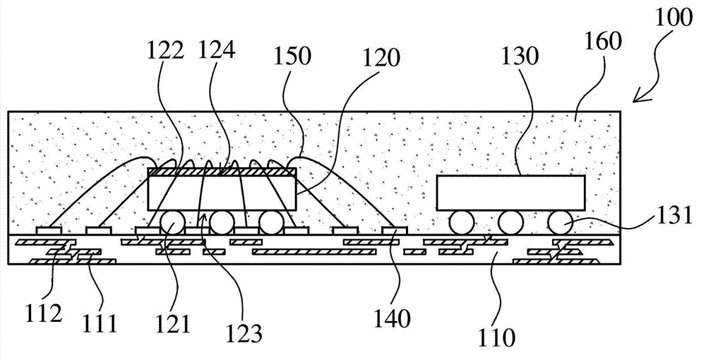
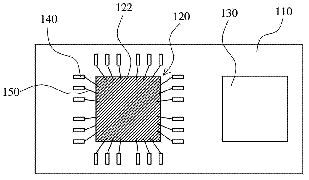
[0022] Please refer to figure 1 and figure 2 , figure 1 shows a cross-sectional view of a semiconductor package structure according to a first embodiment of the present invention, figure 2 A top view of a semiconductor package structure according to a first embodiment of the present invention is shown. The semiconductor package structure 100 of this em...


PUM


Abstract

The invention provides a semiconductor packaging structure and a production method thereof. The method comprises steps of providing a substrate, arranging a plurality of grounding pads on the substrate, arranging a first semiconductor component and a second semiconductor component on the substrate, placing the grounding pads between the first semiconductor component and the second semiconductor component, and connecting a plurality of conductive welding lines to the grounding pads. By the aid of the structure, the conductive welding lines can shield electromagnetic interference effectively.

Description

technical field [0001] The invention relates to a semiconductor packaging structure and a manufacturing method thereof, in particular to a semiconductor packaging structure with an electromagnetic signal shielding structure and a manufacturing method thereof. Background technique [0002] In the semiconductor production process, integrated circuit packaging (IC package) is one of the important steps in the manufacturing process. It is used to protect the IC chip and provide external electrical connections to prevent damage from external forces or environmental factors during transportation and placement. In addition, integrated circuit components also need to be combined with passive components such as resistors and capacitors to form a system in order to perform their intended functions, and electronic packaging (Electronic Packaging) is used to establish the protection and organizational structure of integrated circuit components. Generally speaking, electronic packaging b...

Claims


Application Information

Patent Timeline
Patent Type & Authority Applications(China)
IPC IPC(8): H01L23/552H01L23/31H01L21/56
CPCH01L2224/49112H01L25/0655H01L2224/73257H01L2924/19107H01L24/73H01L2224/16225H01L23/552H01L2224/48227H01L2224/73253H01L2924/3025H01L2924/00
Inventor 沈家贤刘盈男
Owner ADVANCED SEMICON ENG INC
Features
  • R&D
  • Intellectual Property
  • Life Sciences
  • Materials
  • Tech Scout
  • Unparalleled Data Quality
  • Higher Quality Content
  • 60% Fewer Hallucinations
Learn More