Resetting method and resetting control device of register inside chip based on scanning chain

A reset method and scan chain technology, which are applied in the field of scan chain-based chip internal register reset method and reset control device, can solve the problems of chip physical implementation, chip design and implementation, and hardware resource consumption, and achieve simple structure and high performance. Low-impact, physically simple effect

Active Publication Date: 2013-03-13
NAT UNIV OF DEFENSE TECH
View PDF4 Cites 19 Cited by
  • Summary
  • Abstract
  • Description
  • Claims
  • Application Information

AI Technical Summary

Problems solved by technology

This not only consumes a lot of hardware resources, but also brings a certain power consumption overhead of the reset tree, and with the continuous expansion of the scale of digital integrated circuits, the reset tree will continue to increase the complexity of the physical design of the chip, causing great damage to the design and implementation of the chip. Difficulties
[0004] To sum up, the synchronous reset method of the digital integrated circuit in the prior art has a certain

Method used


Image

  • Resetting method and resetting control device of register inside chip based on scanning chain
  • Resetting method and resetting control device of register inside chip based on scanning chain
  • Resetting method and resetting control device of register inside chip based on scanning chain

Examples


Embodiment Construction

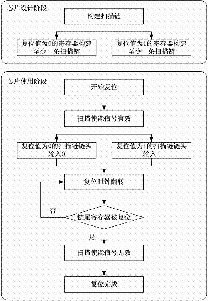
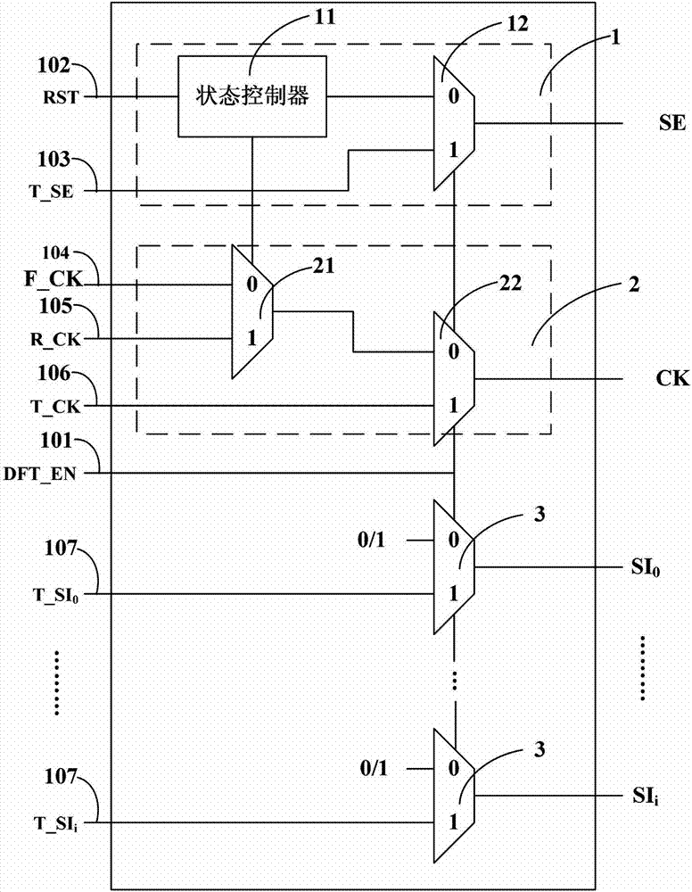
[0020] Such as figure 1 As shown, the implementation steps of the chip internal register reset method based on the scan chain in the embodiment of the present invention are as follows:

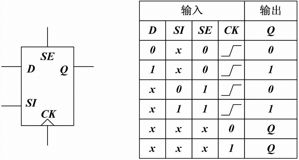
[0021] 1) In the chip design stage, build at least one scan chain for the registers that need to be reset to 0, and at least one scan chain for the registers that need to be reset to 1, and the scan output of the previous register in the same scan chain The scan input of a register is connected;

[0022] 2) In the chip use stage, enable the scan enable signal of each register in the chip, input the reset value 0 at the head of the scan chain composed of the registers that need to be reset to 0, and input the reset value 0 in the scan chain composed of the registers that need to be reset to 1 The scan chain head inputs a reset value of 1 and provides a reset clock to control each scan chain to enter the reset scanning state. Under the control of the input reset clock, the reset value is sequen...


PUM


Abstract

The invention discloses a resetting method and a resetting control device of a register inside a chip based on a scanning chain. The resetting method comprises the steps of: 1) respectively building at least one scanning chain for the register according to a resetting value 0 or 1 in a chip design stage; and 2) setting a scanning enabling signal of each register as valid and writing the resetting value into a head of the scanning chain in a chip use stage. The resetting control device comprises a scanning chain enabling control unit, a scanning chain clock control module and an input data selector which respectively outputs test data or the resetting value to the head of the scanning chain. The input terminal of the resetting control device comprises a test enabling terminal, a resetting signal input end, a test scanning enabling signal/work clock/resetting clock/test clock input end and a plurality of test data input terminals. According to the invention, the inner register of the chip can be efficiently reset so that influence on the performance of a digital integrated circuit chip is low, and the resetting method and the resetting control device have the advantages of high stability, small power consumption, simple structure and is convenient to implement.

Description

technical field [0001] The invention relates to the field of digital integrated circuits, in particular to a scan chain-based chip internal register reset method and a reset control device. Background technique [0002] In a digital integrated circuit, a certain method needs to be used to reset the register so that it has a definite initial state (0 or 1), so as to ensure that the digital integrated circuit can work normally. Register reset methods commonly used in the prior art include synchronous reset and asynchronous reset. [0003] In synchronous reset, when the reset signal is valid, the register is not reset immediately, but when the clock of the register jumps effectively, the register is reset to a fixed initial value. In the synchronous reset structure, the reset signal is used as a data signal to participate in the combinatorial logic operation of the register data input, which increases the number of combinatorial logic stages between registers and has a certain...

Claims


Application Information

Patent Timeline
IPC IPC(8): H03K17/22
Inventor 邓宇龚锐郭御风张明任巨石伟马爱永罗莉窦强王永文
Owner NAT UNIV OF DEFENSE TECH
Why Eureka
Try Eureka