Planar inductor devices
A planar, inductor technology, applied in the direction of inductors, printed inductors, fixed inductors, etc., can solve problems such as broken, damaged ferrite, manual machine winding of conductive wiring, etc.
- Summary
- Abstract
- Description
- Claims
- Application Information
AI Technical Summary
Problems solved by technology
Method used
Image
Examples
Embodiment Construction
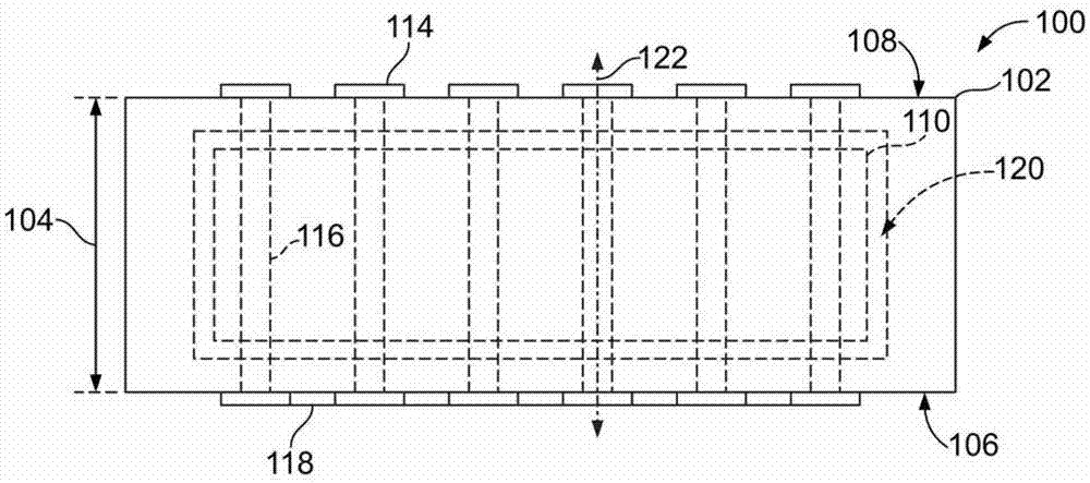
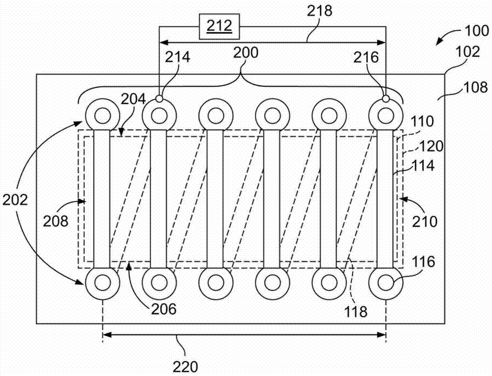
[0033] figure 1 is a side view of one embodiment of a planar inductor device 100 . The device 100 includes a planar substrate 102 in which one or more electronic components of the device 100 are embedded. "Planar" means that the substrate 102 is larger along two vertical dimensions than along a third vertical dimension. The substrate 102 may be a flexible and non-rigid sheet, such as a cured epoxy sheet, or a rigid or semi-rigid board, such as a printed circuit board (PCB) formed of FR-4.
[0034] The substrate 102 has a thickness dimension 104 measured vertically from a lower surface 106 to an opposing upper surface 108 . The thickness dimension 104 can be small, such as 2.5 millimeters or less, 2.0 millimeters or less, 1.0 millimeters or less, or other distances. Alternatively, the thickness dimension 104 may be a larger distance.
[0035] In one embodiment, the substrate 102 includes an interior cavity 120 . The internal cavity 120 may be at least partially filled with...
PUM
| Property | Measurement | Unit |
|---|---|---|
| diameter | aaaaa | aaaaa |
Abstract
Description
Claims
Application Information


