Antistatic structure of liquid crystal panel, manufacturing method thereof, and repairing method of connecting wire
A technology for a liquid crystal panel and a manufacturing method, applied in the directions of static electricity, electrical components, nonlinear optics, etc., can solve problems such as poor connection lines of an array substrate, and achieve the effect of avoiding static electricity
- Summary
- Abstract
- Description
- Claims
- Application Information
AI Technical Summary
Problems solved by technology
Method used
Image
Examples
Embodiment 1
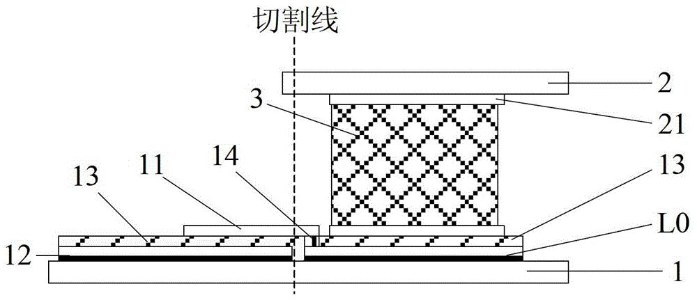
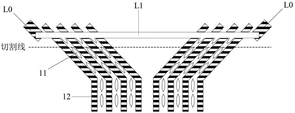
[0035] Such as figure 1 and figure 2 As shown, the antistatic structure of a liquid crystal panel provided by the embodiment of the present invention includes several pointed discharge structures 11, external wires L1 and internal wires L0; several pointed discharge structures 11 and external wires L1 are arranged on the same layer on the array substrate 1 middle;
[0036] Several point discharge structures 11 are located in corresponding areas above the connection lines 12 on the edge of the array substrate 1 , and the number of point discharge structures 11 are separated from the connection lines 12 by an insulating layer 13 . The connecting wires 12 in the embodiment of the present invention are a plurality of side-by-side arrangements in a fan shape, and the connecting wires can be scanning lines or data lines, that is, the antistatic structure provided by the embodiment of the present invention can be used to protect scanning lines, to protect data lines. As a preferr...
Embodiment 2
[0046] The embodiment of the present invention also provides a method for manufacturing an antistatic structure, including the following steps:
[0047] S1: Through a patterning process, a pattern including internal wires is formed on the array substrate.
[0048] As a preferred solution, by means of a patterning process, while forming the scan line pattern on the array substrate, corresponding internal wires can also be formed.
[0049] Specifically, the pattern of the mask plate in the patterning process is changed. On the basis of the original scanning line pattern of the mask plate, the corresponding internal wire pattern is added, and then after conventional exposure, etching and other steps, the Scan line patterns and corresponding internal wires can be formed simultaneously.
[0050] S2: Through a patterning process, a pattern including internal wires is formed on the array substrate.
[0051] This step is similar to step S1. On the basis of the original data line pat...
Embodiment 3
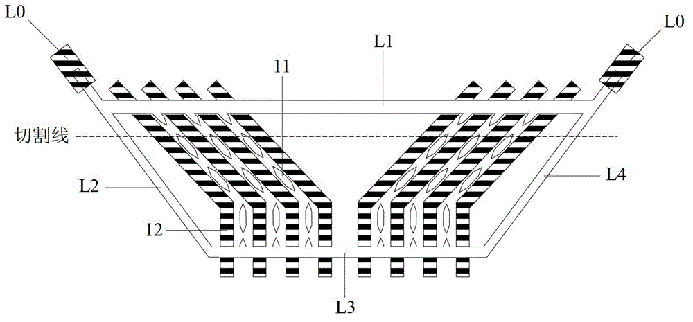
[0059] Such as image 3 As shown, the antistatic structure provided in this embodiment is based on Embodiment 1, and its external wires specifically include a first external wire L1, a second external wire L2, a third external wire L3, and a fourth external wire L4, wherein, The first external lead L1 is located between the cutting line and the sealant, and the third external lead L3 is located outside the cutting line. The first external wire L1, the second external wire L2, the third external wire L3 and the fourth external wire L4 are connected end to end to form a closed loop.
[0060] In this embodiment, the charge on the tip discharge structure 11 can also be transferred to the third outer wire L3, then transferred to the via hole 14 through the second outer wire L2 or the fourth outer wire L4, and finally transferred to the array through the inner wire L0 Electrostatic rings within the substrate. Compared with Embodiment 1, the charge distribution on the closed circui...
PUM
 Abstract
Description
Claims
Application Information


