De-embedding method

A technology of de-embedding and scattering parameters, which is applied to measurement devices, instruments, measuring electricity, etc., can solve the problems of complex de-embedding methods, excessive occupation of vector network analyzers, etc., and achieve the effect of simple method, reduced occupation and remarkable effect.

Active Publication Date: 2013-04-24
SHANGHAI HUAHONG GRACE SEMICON MFG CORP
View PDF12 Cites 22 Cited by
  • Summary
  • Abstract
  • Description
  • Claims
  • Application Information

AI Technical Summary

Problems solved by technology

[0006] However, in the above de-embedding method, after using the vector network analyzer to measure the scattering parameters of the test structure, the open-circuit de-embedding structure and the short-circuit de-embedding structure under multiple test signals of different frequencies, the vector network analyzer is used to measure the open-circuit de-embedding again. The scattering parameters of the embedding structure and the short-circuit de-embedding structure under the test signals of three specific frequencies make the de-embedding method too complicated and occupy too much vector network analyzer

Method used


Image

  • De-embedding method
  • De-embedding method
  • De-embedding method

Examples


Embodiment Construction

[0042] The technical solutions of the present invention will be clearly and completely described below with reference to the accompanying drawings through specific embodiments. Obviously, the described embodiments are only a part of the embodiments of the present invention, but not all of them. According to these embodiments, all other implementations that can be obtained by a person of ordinary skill in the art without creative efforts fall within the protection scope of the present invention.

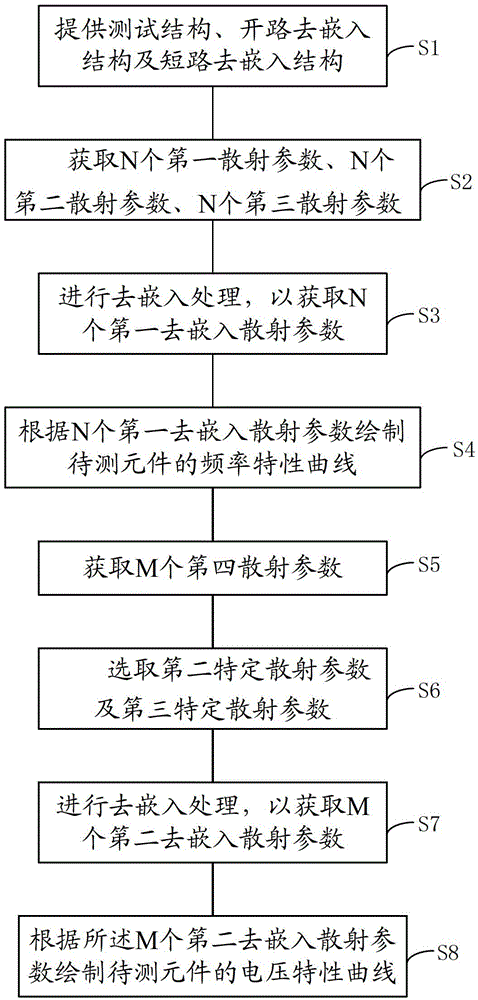
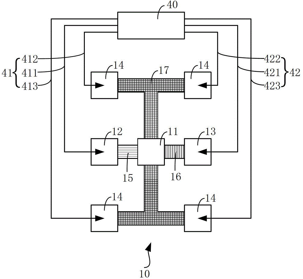
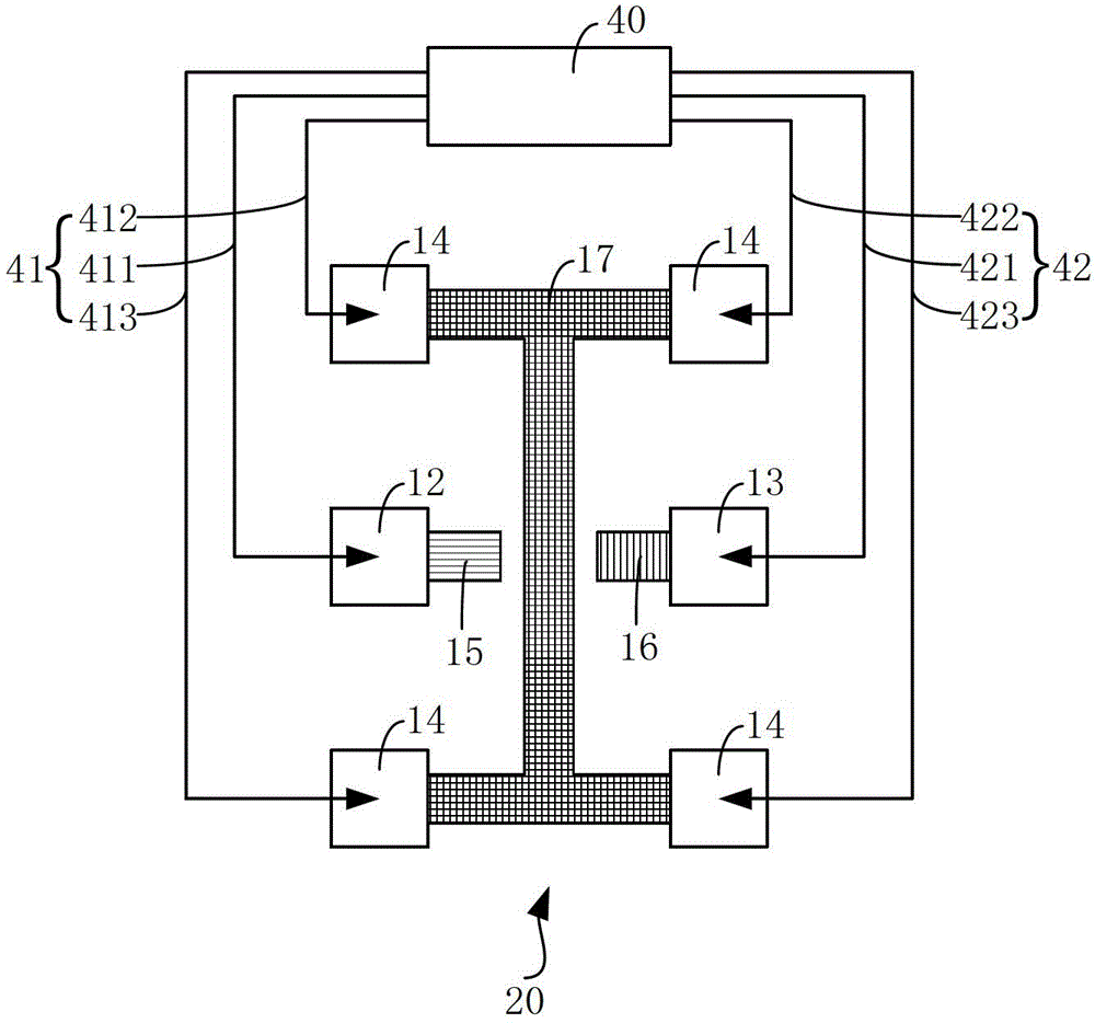
[0043] figure 1 is a flow chart of the de-embedding method in an embodiment of the present invention, figure 2 is a schematic structural diagram of the test structure in an embodiment of the present invention, image 3 is a schematic structural diagram of an open-circuit de-embedding structure in an embodiment of the present invention, Figure 4 is a schematic structural diagram of a short-circuit de-embedding structure in an embodiment of the present invention, which is combined b...


PUM


Abstract

The invention discloses a de-embedding method. A scattering parameter under a testing signal of a plurality of different frequencies of a vector network analysis meter surveying testing structure, an open circuit de-embedding structure and a short circuit de-embedding structure is used. A plurality of scattering parameters of the open circuit de-embedding structure and a plurality of scattering parameters of the short circuit de-embedding structure are stored at the same time. The scattering parameters under the specific frequency of the testing signal frequency of the open circuit de-embedding structure are not needed to be surveyed and the scattering parameters under the specific frequency of the testing signal frequency of the short circuit de-embedding structure are not needed to be surveyed when de-embedding scattering parameters under the specific frequency of the testing signal frequency of a to-be tested component obtained follow-up. The de-embedding method is simple and occupation of the vector network analysis meter is reduced. The specific frequency is needed to be changed many times when voltage characteristics of the to-be tested component is analyzed comprehensively, thus effect of a technical scheme is prominent.

Description

technical field [0001] The present invention relates to the field of testing of semiconductor components, in particular to a method for de-embedding. Background technique [0002] Integrated circuits formed on semiconductor substrates include a number of active and passive elements, such as resistors, inductors, capacitors, transistors, amplifiers, and the like. The device is fabricated according to design specifications that define the desired electrical characteristics of the device. In general, it is desirable to confirm that each component meets its specific design specifications, however after the components are integrated into an integrated circuit, individual components are often not easily tested. Thus, stand alone copies of individual components in an integrated circuit are fabricated on a wafer, and electrical characteristics of the individual copies are then measured. The independent replica element is manufactured by the same process as the element in the integ...

Claims


Application Information

Patent Timeline
Patent Type & Authority Applications(China)
IPC IPC(8): G01R31/27
Inventor 廖梦星
Owner SHANGHAI HUAHONG GRACE SEMICON MFG CORP
Why Eureka
Try Eureka