Interface circuit and achievement method for limiting output port voltage slew rate

A technology of output terminal voltage and interface circuit, which is applied in the direction of logic circuit connection/interface layout, logic circuit coupling/interface using field effect transistors, etc. It can solve the problem that the interface circuit cannot take into account the limitation of voltage slew rate and high transmission rate, etc. To achieve the effect of increasing the transmission rate

Active Publication Date: 2013-04-24
SHENZHEN STATE MICRO TECH CO LTD
View PDF7 Cites 13 Cited by
  • Summary
  • Abstract
  • Description
  • Claims
  • Application Information

AI Technical Summary

Problems solved by technology

[0003] The present invention is to solve the requirement that the existing interface circuit cannot take into account both the limitation of the voltage slew rate and the high transmission rate, and proposes a circuit that can limit the voltage slew rate and output current and has a high data transmission rate

Method used


Image

  • Interface circuit and achievement method for limiting output port voltage slew rate
  • Interface circuit and achievement method for limiting output port voltage slew rate
  • Interface circuit and achievement method for limiting output port voltage slew rate

Examples


Embodiment Construction

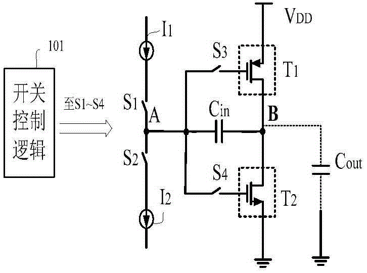
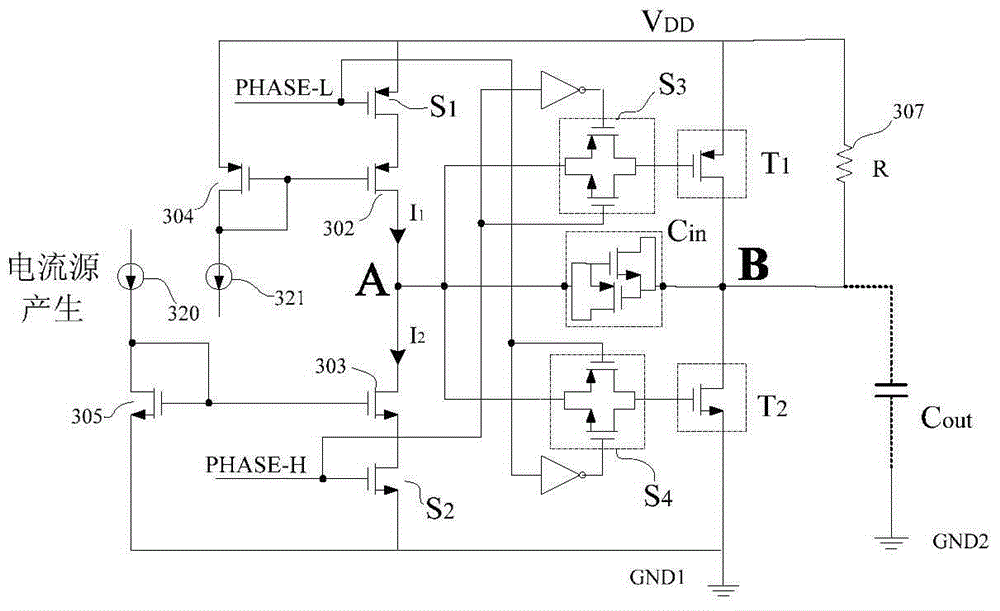
[0018] An interface circuit that limits the voltage slew rate at the output, see figure 1 The circuit principle shown includes: a current source I1, a current sink I2, a first switch S1 and a second switch S2 connected in series with the current source I1 and the current sink I2 respectively, and the switches connected in series between the power supply and the ground The first PMOS transistor T1 and the first NMOS transistor T2, the third switch S3 connected to the gate of the first PMOS transistor T1, the fourth switch S4 connected to the gate of the first NMOS transistor T2, the first PMOS transistor T1 and the first NMOS transistor The connection point of T2 is used as the output end of the interface circuit; the current source I1 branch and the current sink I2 branch are connected at the common end A, and the common end is connected to the other end of the third switch S3 and the fourth switch S4; the common end is connected to the output An on-chip capacitor Cin is conne...


PUM


Abstract

The invention discloses an interface circuit and achievement method for limiting output port voltage slew rate. The interface circuit and achievement method for limiting output port voltage slew rate comprise a first switch and a second switch respectively connected with a current source and a current sink in series, a first P-channel Metal Oxide Semiconductor (PMOS) pipe and a first N-channel metal oxide semiconductor (NMOS) pipe which are sequentially in series connection and arranged between a power and ground, a third switch connected with a gate electrode of the first PMOS pipe and a fourth switch connected with a gate electrode of the first NMOS pipe, wherein the connection point of the first PMOS pipe and the first NMOS pipe acts as an output port of the interface circuit; a current source branch and a current sink branch are connected on the position of a public port, and the public port is connected with the other end of the third switch and the fourth switch; an in-chip capacitor is connected between the public port and the output end. The interface circuit limiting output port voltage slew rate and achievement method further comprise a logic control unit respectively connected with control electrodes of the first switch, the second switch, the third switch and the fourth switch to control on-off of the control electrodes. The interface circuit and achievement method for limiting output port voltage slew rate can effectively limit voltage slew rates and output current of the output port of the interface circuit, and play roles of decreasing electro-magnetic interference (EMI), protecting the interface circuit and improving transmission rates of the interface circuit.

Description

technical field [0001] The invention relates to an interface circuit for transmitting data, in particular to an interface circuit for limiting the voltage slew rate of an output terminal and a realization method thereof. Background technique [0002] The interface circuit is an indispensable and important part in data transmission. In the application of the interface circuit, if a traditional inverter is used to drive the output port, there will be a situation where the output transient current is too large when switching between high and low levels. If not limited, such a sudden change in current will deteriorate the EMI characteristics of the interface circuit, and excessive current may damage the output device of the interface circuit. The usual limiting method is to connect a resistive device in series with the output device; or only use a pull-up and pull-down resistor as the output device to play the role of pull-up or pull-down, and also play the role of current limit...

Claims


Application Information

Patent Timeline
Patent Type & Authority Applications(China)
IPC IPC(8): H03K19/0185
Inventor 吴晓勇王新亚
Owner SHENZHEN STATE MICRO TECH CO LTD
Why Eureka
Try Eureka