Biopolymer optical analysis device and method

一种生物聚合物、解析装置的技术,应用在特性进行解析的装置领域,能够解决操作复杂等问题,达到识别能力高的效果

Active Publication Date: 2013-04-24
HITACHI HIGH-TECH CORP
View PDF12 Cites 16 Cited by
  • Summary
  • Abstract
  • Description
  • Claims
  • Application Information

AI Technical Summary

Problems solved by technology

That is, there is a problem that the device configuration and operation are complicated

Method used


Image

  • Biopolymer optical analysis device and method
  • Biopolymer optical analysis device and method
  • Biopolymer optical analysis device and method

Examples


Embodiment 1

[0098] [Example 1] Characteristic Analysis of Nanopore Chip and Biopolymer Using the Nanopore Chip

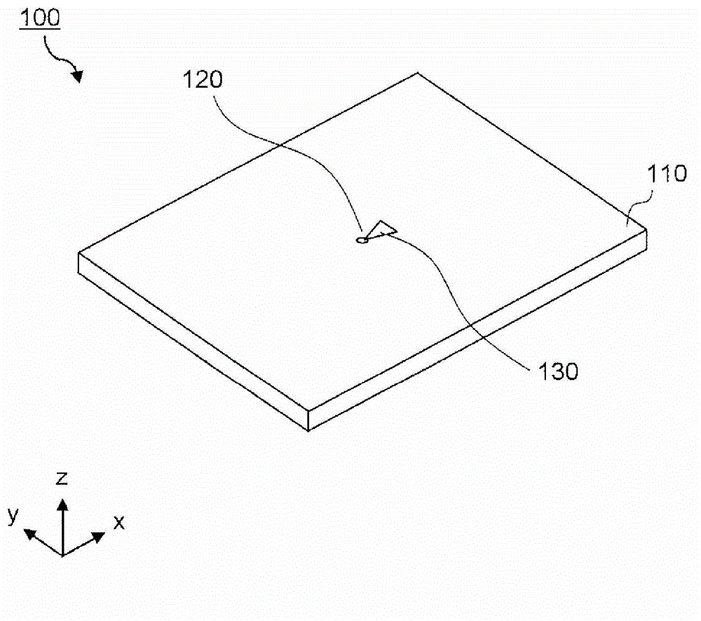
[0099] use figure 1 Now, an example of the configuration of the nanopore chip for biopolymer property analysis of the present invention will be described. figure 1 It is a schematic diagram of the nanopore chip 100 for analyzing the properties of the biopolymer in this example. As shown in the figure, the nanopore chip 100 is composed of a substrate 110, a nanopore 120, a conductive thin film 130, and the like. As shown in the figure, the plane parallel to the widest surface of the substrate 110 (hereinafter referred to as the substrate surface) is defined as the xy plane, the direction connecting the conductive thin film 130 and the nanopore 120 is defined as the x axis, and the direction perpendicular to the xy plane is defined as The direction is defined as the z-axis. The nanopore 120 is formed approximately perpendicular to the substrate surface, in other words, the cen...

Embodiment 2

[0137] [Example 2] Structure of multi-nanopore analysis device

[0138] use Figure 11 An example of the configuration of the multi-nanopore chip for biopolymer property analysis of the present invention will be described. Figure 11 It is a schematic diagram of the multi-nanopore chip 1100 for analyzing the properties of the biopolymer in Example 2. As shown in the figure, the multi-nanohole chip 1100 is composed of a substrate 1110, nanopores 1120, 1121, conductive thin films 1130a, 1130b, 1131a, 1131b, and the like. As shown in the figure, the multi-nanohole chip 1100 of this embodiment has the unit structure of the above-mentioned modified example in which a plurality of nanopores and conductive thin films facing each other are formed on one substrate 1110, that is, Figure 10 The unit structure exemplified in .

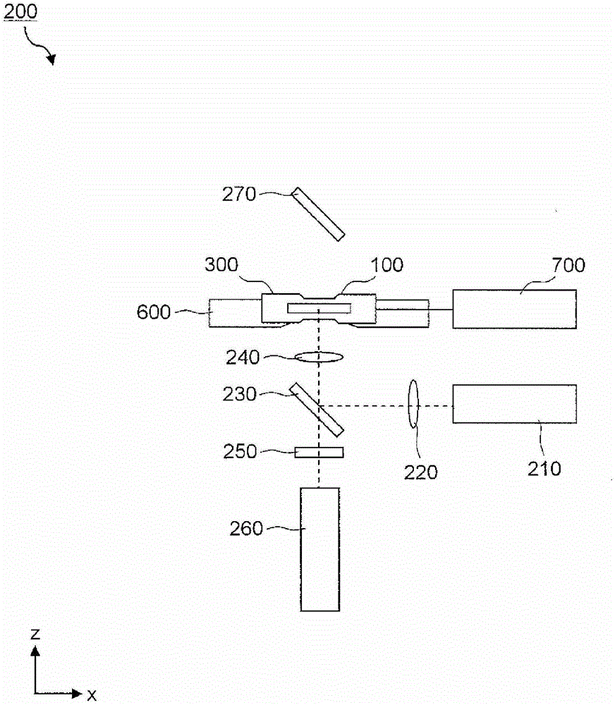
[0139] Next, use Figure 12 An example of the configuration of the biopolymer property analysis device in this example will be described. Figure 12 It is a...

Embodiment 3

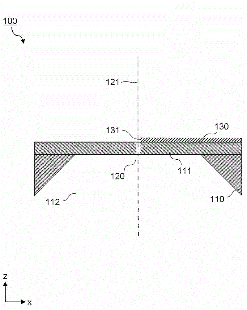
[0148] [Example 3] Nanopore chip of sandwich structure

[0149] use Figure 13 An example of the configuration of the nanopore chip for analyzing the properties of the biopolymer according to the present invention will be described. Figure 13 It is a schematic enlarged view of the xz cross-section including the central axis 121 of the nanopore 120 of the nanopore chip 100 b of the third embodiment. The substrate surface of the substrate 110 above the z-axis has a thin film portion 111a, has conductive thin films 130a and 130b thereon, and further has a thin film portion 111b thereon. Other modification examples with embodiment 1 ( Figure 10 )same.

[0150] The fabrication method of the nanopore chip 100b of the present embodiment 3 is similar to that of the embodiment 1 (modified example), but after forming the patterns of the conductive thin films 130a, 130b by EB etching, a SiO film with a film thickness of about 20nm is formed by sputtering. 2The formed thin film port...


PUM


Abstract

The present invention provides a device and method for analysing the characteristics of a biopolymer with excellent mechanical stability, high spatial resolution and sensitivity using a simple device construction. Specifically, the Raman scattered light of a biopolymer is measured and the properties of monomer units forming the biopolymer are analysed by using a biopolymer property analysis chip (100a) characterized by comprising: a solid substrate (110); at least one nanopore (120) disposed in the solid substrate (110); and one or more electrically conductive thin films (130a, 130b) disposed on the solid substrate (110). The biopolymer property analysis chip (100a) is characterized in that the electrically conductive thin films (130a, 130b) are disposed in the part of the solid substrate (110) where the nanopore (120) is formed and a biopolymer which has penetrated into the nanopore (120) is caused to generate Raman scattered light by means of irradiation with external light.

Description

technical field [0001] The present invention relates to a device and method for analyzing properties of biopolymers using a chip-like device having nanometer-sized pores. In particular, the present invention relates to an apparatus, device, and method for performing characteristic analysis by forming a near field in a nanopore chip and optically detecting biopolymers such as nucleic acids without labeling. Background technique [0002] As a method to realize a more advanced next-generation DNA sequencer, technology using nanopores has attracted attention. It is considered that the major feature of the nanopore method is that it can be analyzed without labeling DNA, in other words, without using reagents such as enzymes and fluorescent dyes. Nanopores are broadly classified into two types according to their formation methods. One is a so-called biological nanopore in which a channel protein forming a nanometer-sized opening (hereinafter referred to as a "nanopore") is embed...

Claims


Application Information

Patent Timeline
Patent Type & Authority Applications(China)
IPC IPC(8): G01N21/65B82Y5/00B82Y15/00C12N15/09G01N37/00
CPCG01J3/0267B82Y15/00G01N33/48721G01N21/65B82Y5/00G01N21/658C12Q1/6869C12Q2565/631C12Q2565/632
Inventor 小泽理穴泽隆赤堀玲奈高桥智大浦刚木口雅史
Owner HITACHI HIGH-TECH CORP
Why Eureka
Try Eureka