Production method of thick-electrode device

A production method and electrode technology, which is applied in the manufacture of inductors/transformers/magnets, electrical components, cables/conductors, etc., can solve the problems of increased electrode slurry consumption, sintering cracks, and increased product costs, and reduce DC resistance , the effect of reducing the width

Inactive Publication Date: 2013-05-01
SHENZHEN SUNLORD ELECTRONICS
View PDF3 Cites 10 Cited by
  • Summary
  • Abstract
  • Description
  • Claims
  • Application Information

AI Technical Summary

Problems solved by technology

However, the low-mesh screen cannot be applied to products with small electrode widths, and the printing quality of the electrodes cannot be guaranteed by the method of multiple printing: due to multiple printings of the electrodes, the electrodes will become wider and the lines will be less straight
These two methods a

Method used


Image

  • Production method of thick-electrode device
  • Production method of thick-electrode device
  • Production method of thick-electrode device

Examples


Embodiment 1

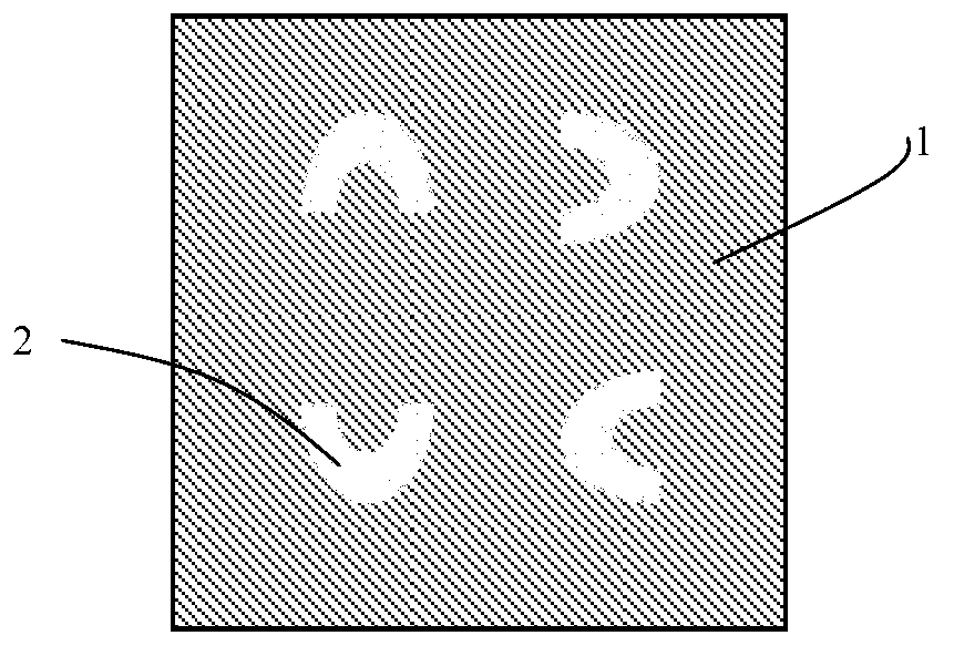
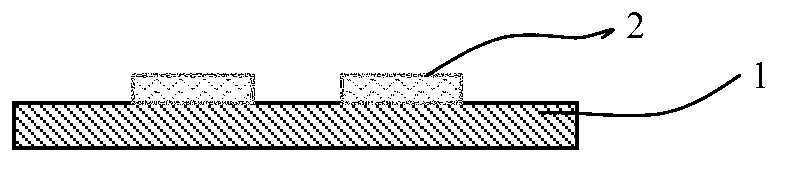
[0044] This embodiment provides a method for manufacturing a thick electrode device, which is carried out according to the above steps, wherein the thickness of the electrode paste 2 printed on the first ceramic substrate 1 and the film 3 with a release function in step 1) is 25 μm; the pressure of the laminator in step 2) is 0.15 tons / square inch, and the temperature is 30°C; the pressure of the laminator in step 3) is 0.15 tons / square inch, and the temperature is 30°C, and the third ceramic substrate is formed After 7 and electrode slurry 6, the thickness of the electrode is 36 μm at this time, that is, a complete device structure is formed; the deglue curve in step 4) is: firstly heat up to 200°C after 20 hours, then heat up to 400°C, keep warm 10 hours, and finally cool down naturally; the sintering curve in step 5) is: firstly, the temperature is raised to 700°C in 10 hours, then to 900°C, kept for 5 hours, and the temperature is naturally lowered to obtain the thick elect...

Embodiment 2

[0046] This embodiment provides a method for manufacturing a thick electrode device, which is carried out according to the above steps, wherein the thickness of the electrode paste 2 printed on the first ceramic substrate 1 and the film 3 with a release function in step 1) is 30 μm; the pressure of the laminator in step 2) is 0.2 tons / square inch, and the temperature is 35°C; the pressure of the laminator in step 3) is 0.2 tons / square inch, and the temperature is 35°C, and the third ceramic substrate is formed 7 and electrode paste 6, the thickness of the electrode at this time is 41 μm, and the third ceramic substrate 7 is printed on the third ceramic substrate 7 according to the required electrode pattern stacking sequence and the steps 1) to 3) are laminated 5 times and the ceramic substrate is formed. A complete device structure; the deglue curve in step 4) is: first heat up to 300°C for 25 hours, then heat up to 350°C, keep warm for 20 hours, and cool down naturally; the s...

Embodiment 3

[0048]This embodiment provides a method for manufacturing a thick electrode device, which is carried out according to the above steps, wherein the thickness of the electrode paste 2 printed on the first ceramic substrate 1 and the film 3 with a release function in step 1) is 28 μm; the pressure of the lamination machine in step 2) is 0.25 tons / square inch, and the temperature is 25°C; the pressure of the lamination machine in step 3) is 0.25 tons / square inch, and the temperature is 25°C, and the third ceramic substrate is formed 7 and electrode paste 6, the thickness of the electrode at this time is 38 μm, and the third ceramic substrate 7 is printed on the third ceramic substrate 7 in accordance with the required electrode pattern stacking sequence for 9 times and the laminated ceramic substrate is formed. A complete device structure; the deglue curve in step 4) is: firstly, the temperature is raised from room temperature to 180°C for 22 hours, then the temperature is raised t...


PUM

PropertyMeasurementUnit
Thicknessaaaaaaaaaa
Thicknessaaaaaaaaaa
Thicknessaaaaaaaaaa

Abstract

The invention relates to a production method of a thick-electrode device, and the production method comprises the following steps of utilizing screen meshes with the same patterns to be printed with electrode paste on a first ceramic substrate and a film with a releasing function; utilizing the obtained film which is printed with the electrode paste to be laminated onto a second ceramic substrate, and removing the film to obtain the second ceramic substrate with the electrode paste; inverting the first ceramic substrate which is printed with the electrode paste onto the second ceramic substrate with the electrode paste to be aligned and laminated for the electrode patterns to form a third ceramic substrate; discharging the glue; and sintering. Due to the adoption of the production method of the thick-electrode device, the width of the electrode is reduced, while the production of a thick electrode is realized, the direct-current resistance of the device is effectively reduced, and the consumption of the electrode paste can be reduced on the premise of guaranteeing the performance of the device.

Description

technical field [0001] The invention relates to a manufacturing method of a thick electrode device. Background technique [0002] In the past, the method used to make conductive devices such as inductors with thick electrodes and small DC resistance is mainly to use low-mesh screens to print or to use non-stop multiple printing methods to achieve. However, the low-mesh screen cannot be applied to products with small electrode widths, and the printing quality of the electrodes cannot be guaranteed by the method of multiple printing: due to the multiple printing of the electrodes, the electrodes will become wider and the lines will be less straight. These two methods are likely to make the width of the electrode larger than expected, and if the electrode width is too large, the problem of sintering cracking will easily occur. At the same time, since the electrode width becomes larger, the consumption of electrode paste will also increase, which directly leads to an increase i...

Claims


Application Information

Patent Timeline
IPC IPC(8): H01B13/00H01F41/00
Inventor 陆达富王清华曾向东
Owner SHENZHEN SUNLORD ELECTRONICS
Why Eureka
Try Eureka