Manufacturing process for copper-based printed circuit board with embedded circuits

A printed circuit board and manufacturing process technology, which is applied in the direction of assembling printed circuits with electrical components, can solve problems such as short life, poor stability, and low heat dissipation efficiency, and achieve the effects of prolonging service life, avoiding limited life, and improving reliability

Active Publication Date: 2013-05-01
SHENZHEN WUZHU TECH
View PDF2 Cites 10 Cited by
  • Summary
  • Abstract
  • Description
  • Claims
  • Application Information

AI Technical Summary

Problems solved by technology

[0006] Aiming at the technical problems of low heat dissipation efficiency, poor stability and short service life of the existing printed circuit board, the present invention provides a copper-based embedded circuit manufacturing process with high heat dissipation efficiency, good stability and long service life.

Method used


Image

  • Manufacturing process for copper-based printed circuit board with embedded circuits
  • Manufacturing process for copper-based printed circuit board with embedded circuits
  • Manufacturing process for copper-based printed circuit board with embedded circuits

Examples


Embodiment Construction

[0021] Specific embodiments of the present invention will be described in detail below in conjunction with the accompanying drawings.

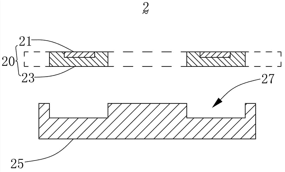
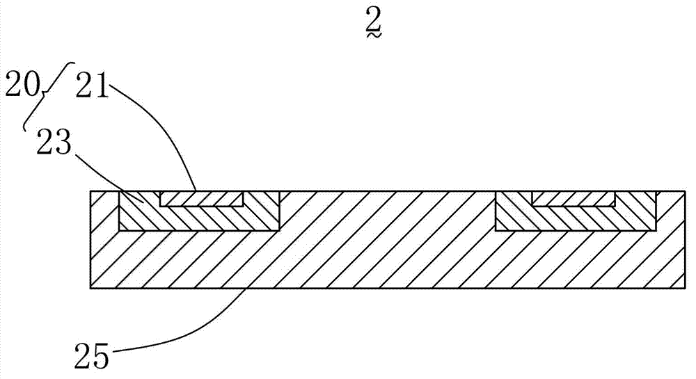
[0022] Figure 2 to Figure 4 Disclosed is a preferred embodiment of the printed circuit board structure and manufacturing process of copper-based embedded circuits of the present invention.

[0023] Please also see figure 2 and image 3 . in figure 2 It is an exploded schematic diagram of the manufacturing process structure of a copper-based printed circuit board with embedded circuits in the present invention. image 3 yes figure 2 A schematic diagram of the assembly of a printed circuit board manufacturing process structure with embedded circuits in a copper base is shown. The copper-based printed circuit board 2 includes a copper-clad laminate 20 with copper removed from the bottom, a heat sink 25 and a plurality of electronic components (not shown) disposed on the surface of the substrate 20 .

[0024] The copper clad laminate 20...


PUM


Abstract

The invention provides a manufacturing process for a copper-based printed circuit board with embedded circuits. The manufacturing process comprises the following steps: a heat dissipation plate is provided, and grooves are etched in the surface of the heat dissipation plate; a copper-clad plate is provided; the bottom surface of the copper-clad plate is glued after copper removal; the copper-clad plate is hollowed out, and non hollowed-out areas of the copper-clad plate are arranged in the grooves; the copper-clad plate and the heat dissipation plate are combined by pressing, and a top surface is ground flush; and graph circuits are manufactured on the top surface of the copper-clad plate to form the copper-based printed circuit board with embedded circuits. According to the manufacturing process for the copper-based printed circuit board with the embedded circuits, the copper-clad plate is embedded in the grooves of the heat dissipation plate, electronic elements can be directly contacted with the heat dissipation plate for rapid heat dissipation, the reliability of the electronic elements is improved, the entire working stability of an electronic product is improved, and the service life of the electronic product is prolonged.

Description

technical field [0001] The invention relates to a manufacturing process of a printed circuit board with embedded circuits in a copper base. Background technique [0002] With the development of light, thin, small, high-density and multi-functional electronic products, the assembly density and integration of electronic components on printed circuit boards are getting higher and higher, and the power consumption is increasing. The heat dissipation requirements of printed circuit boards Higher and higher. [0003] see figure 1 , is a schematic diagram of the side structure of a printed circuit board in the prior art. The printed circuit board 1 includes a circuit layer 11 , an insulating layer 13 , a metal plate 15 and electronic components (not shown in the figure), and the circuit layer 11 , the insulating layer 13 and the metal plate 15 are sequentially stacked. The circuit layer 11 is separated from the metal plate 15 by the insulating layer 13 , and a plurality of elect...

Claims


Application Information

Patent Timeline
Patent Type & Authority Applications(China)
IPC IPC(8): H05K3/30
Inventor 徐学军
Owner SHENZHEN WUZHU TECH
Why Eureka
Try Eureka