Wafer cutting method

A cutting method and a wafer technology, which are applied in the fields of electrical components, fine working devices, semiconductor/solid-state device manufacturing, etc., can solve the problems that the bonded wafer 100 cannot be firmly fixed and affect the cutting accuracy, etc., to achieve The effect of improving cutting stability and precision

Active Publication Date: 2015-03-25
HIMAX TECH LTD
View PDF10 Cites 0 Cited by
  • Summary
  • Abstract
  • Description
  • Claims
  • Application Information

AI Technical Summary

Problems solved by technology

Since these solder balls 130 will affect the adhesion between the dicing adhesive film 140 and the bonded wafer 100, it is easy to cause the bonded wafer 100 to be unable to be firmly fixed during the dicing process, which will also affect the accuracy of dicing.

Method used


Image

  • Wafer cutting method
  • Wafer cutting method
  • Wafer cutting method

Examples


Embodiment Construction

[0033] Embodiments of the invention will now be described in detail by way of example depicted in the accompanying drawings. However, it is not intended to limit these embodiments to the implementations described below, and the implementations herein are provided so that readers can easily and completely understand the scope and spirit of the present invention. In the illustrations, the size and thickness of some elements and structures are exaggerated for clarity.

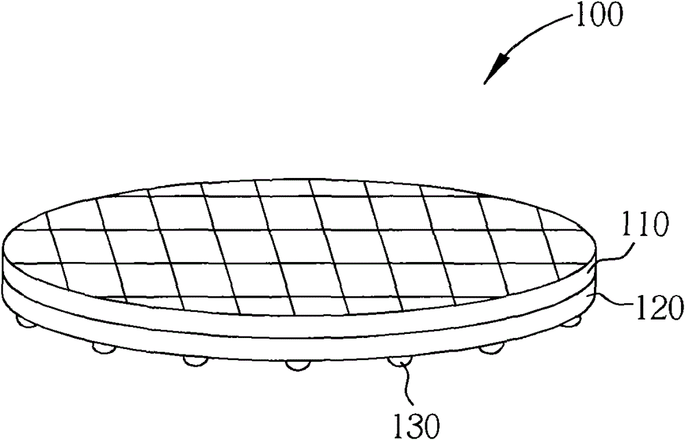
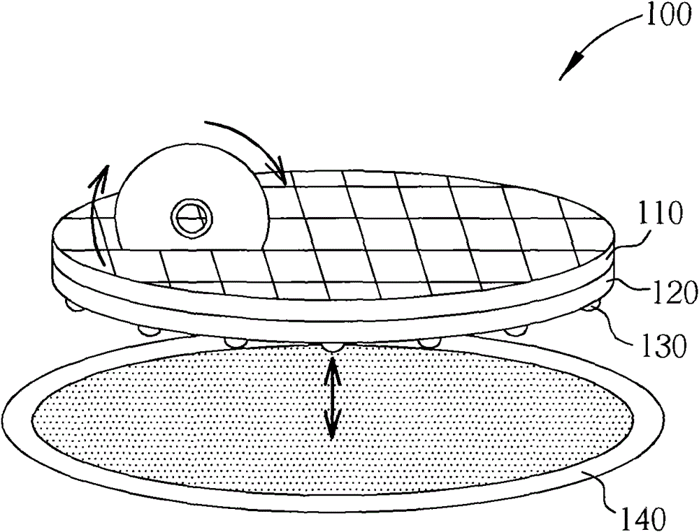
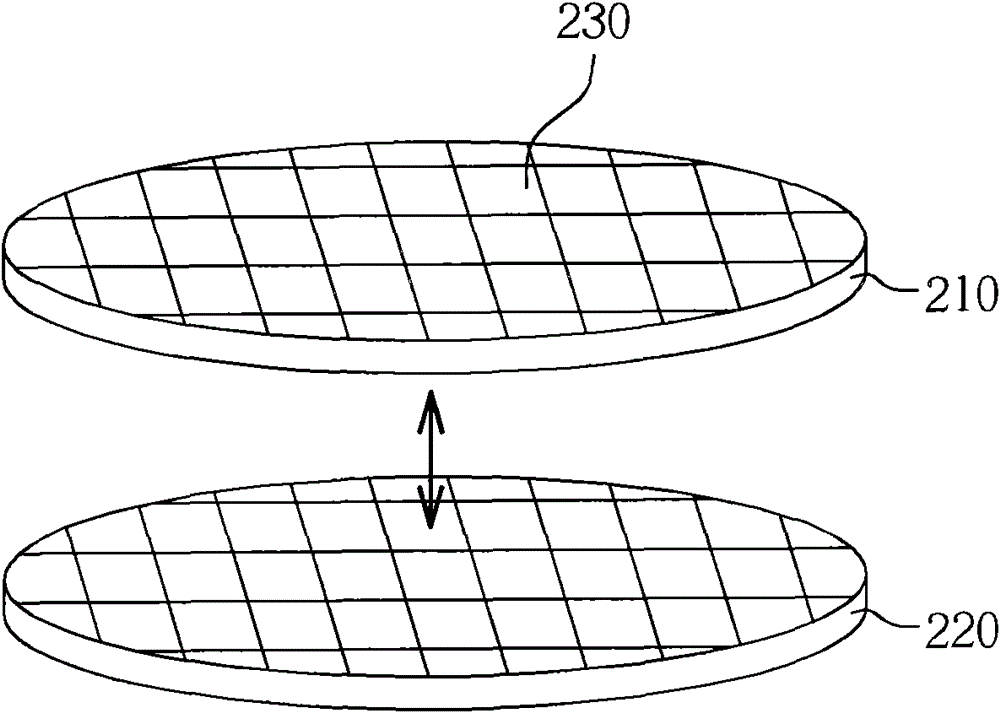
[0034] Please refer to Figure 3 to Figure 11 , which sequentially depict the steps of the wafer cutting method of the present invention. First please also refer to image 3 and Figure 4 , which depicts a schematic diagram of the wafer-to-wafer bonding step in the flow of the wafer dicing method according to the present invention. The object of the wafer dicing method of the present invention is mainly a single wafer or a structure formed by bonding multiple wafers, which is generally referred to as a bonded ...


PUM


Abstract

A wafer cutting method includes that a first wafer and a second wafer are combined to form a combined wafer, half cutting action is performed on the first surface of the combined wafer, a tin ball is arranged on the second surface of the combined wafer, and cutting action is performed on the second surface of the combined wafer. Adhesion between a cutting adhesive film and a wafer combining structure in a particle cutting step cannot be influenced by a protruding tin ball structure through a half cutting process and changing of order of a tin ball formation steps, and yield and precision of a subsequent cutting process are improved further.

Description

【Technical field】 [0001] The present invention relates generally to a wafer dicing method, and more particularly to a dicing method for bonding wafer structures at the wafer level. 【Background technique】 [0002] Epitaxy and coating processes are widely used in the manufacturing process of semiconductor components and optoelectronic components to form various layer structures. Generally speaking, to grow another different material on one material, the degree of matching between the atomic lattices of the two must be considered. When a stress field is generated, most of the defects or dislocations will be concentrated at this type of interface, which will lead to problems such as threading dislocation in the subsequent coating film or epitaxial structure, which will seriously affect the performance of the device. In recent years, in order to solve the above-mentioned problems such as lattice size mismatch and tunneling dislocation during coating epitaxy. Wafer-to-wafer bond...

Claims


Application Information

Patent Timeline
Patent Type & Authority Patents(China)
IPC IPC(8): H01L21/304B28D5/00
Inventor 黄腾德
Owner HIMAX TECH LTD
Why Eureka
Try Eureka