Magnetron sputtering source and magnetron sputtering equipment

A technology of magnetron source and magnetron, which is applied in the field of semiconductors, can solve the problems that the target utilization rate needs to be improved, and the movement speed is difficult to control, so as to achieve the effect of improving the target material utilization rate, reducing the generation of particles, and facilitating control

Active Publication Date: 2014-12-17
BEIJING NAURA MICROELECTRONICS EQUIP CO LTD
View PDF5 Cites 0 Cited by
  • Summary
  • Abstract
  • Description
  • Claims
  • Application Information

AI Technical Summary

Problems solved by technology

[0006] Therefore, it is difficult to control the movement speed of the drive mechanism to drive the magnetron to scan different positions of the target, and the utilization rate of the target needs to be improved

Method used


Image

  • Magnetron sputtering source and magnetron sputtering equipment
  • Magnetron sputtering source and magnetron sputtering equipment
  • Magnetron sputtering source and magnetron sputtering equipment

Examples


Embodiment Construction

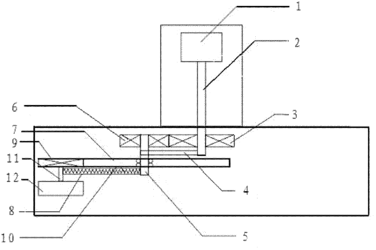
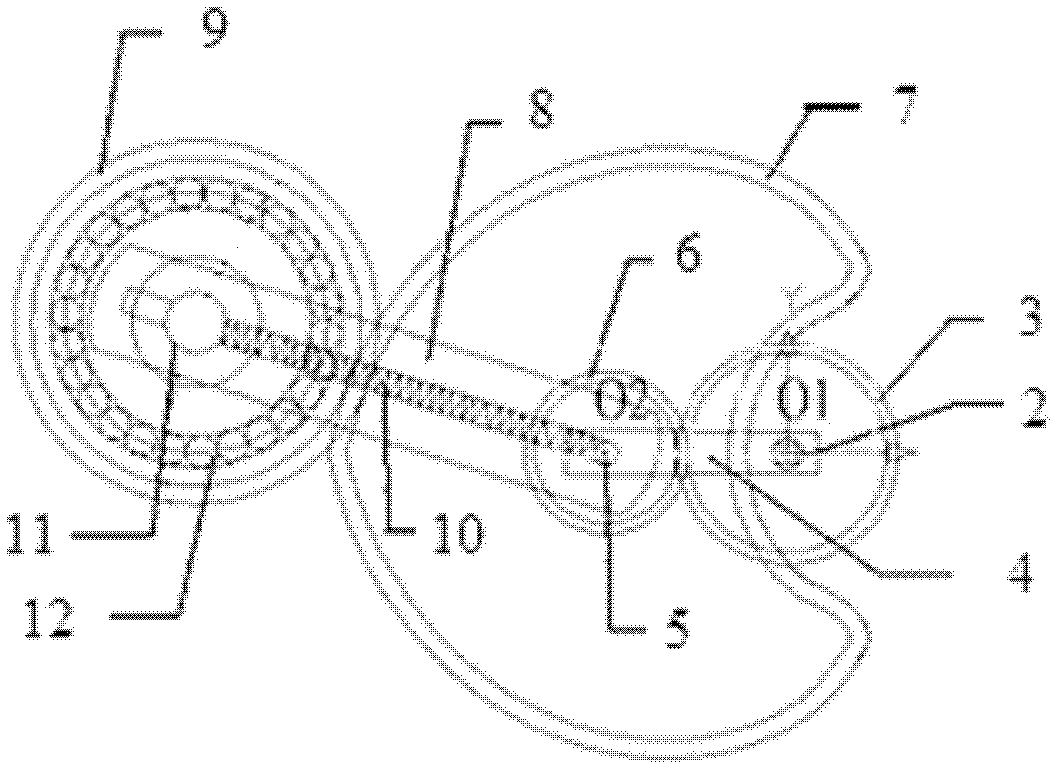
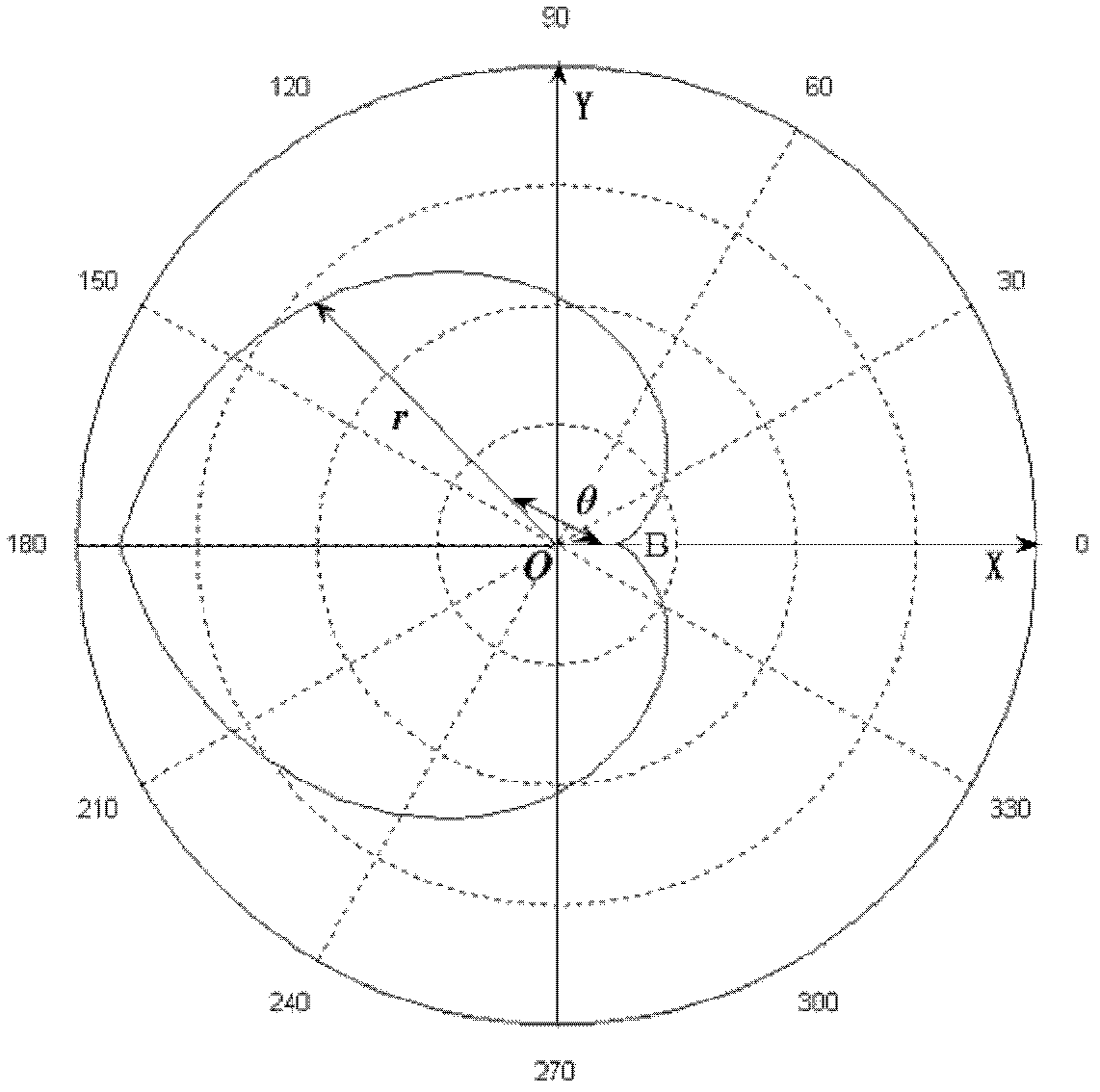
[0039] Embodiments of the present invention are described in detail below, examples of which are shown in the drawings, wherein the same or similar reference numerals designate the same or similar elements or elements having the same or similar functions throughout. The embodiments described below by referring to the figures are exemplary only for explaining the present invention and should not be construed as limiting the present invention.

[0040] In describing the present invention, it should be understood that the terms "center", "longitudinal", "transverse", "upper", "lower", "front", "rear", "left", "right", " The orientations or positional relationships indicated by "vertical", "horizontal", "top", "bottom", "inner", "outer", etc. are based on the orientation or positional relationships shown in the drawings, and are only for the convenience of describing the present invention and simplifying Describes, but does not indicate or imply that the device or element referred...


PUM


Abstract

The invention discloses a magnetron sputtering source and magnetron sputtering equipment with the magnetron sputtering source. The magnetron sputtering source comprises a target material, a magnetron located above the target material, and a scanning mechanism which is connected to the magnetron and is used for controlling the magnetron to move above the target material. The scanning mechanism comprises a driver, a driving shaft, a driving gear, a connection rod, a driven shaft, a driven gear, a cam, a guide rail, a roller and an elastic component. Through adjustment of a distance between the driving shaft and the driven shaft, when the magnetron moves around the cam, a scanning speed of the magnetron at the periphery and the center of the target material is adjusted so that the etching depth of the outer ring of the target material is increased and particles produced in film deposition are reduced and film uniformity and a target material utilization rate are improved. The magnetron sputtering source has the advantages of stable structure, smooth transmission, simple operation and good practicality.

Description

technical field [0001] The invention relates to the technical field of semiconductors, in particular to a magnetron source and a magnetron sputtering device with the magnetron source. Background technique [0002] Magnetron sputtering, also known as physical vapor deposition, is a widely used method for depositing metal layers and related materials in the fabrication of integrated circuits. [0003] Image 6 A typical magnetron sputtering device is shown, wherein a high vacuum process chamber is defined inside the chamber body 9', the sputtered target material 10' is set on the top of the chamber body 9', and the upper cover 11' is set On the target 10', the spacer 11' and the target 10' are filled with deionized water 12', the electrostatic chuck 8' carrying the wafer 7' is set in the high vacuum process chamber, and the pumping chamber 6' is connected with the high vacuum process chamber. The lower part of the vacuum process chamber is connected. [0004] In order to imp...

Claims


Application Information

Patent Timeline
Patent Type & Authority Patents(China)
IPC IPC(8): C23C14/35
Inventor 李杨超刘旭
Owner BEIJING NAURA MICROELECTRONICS EQUIP CO LTD
Why Eureka
Try Eureka