Ion implantation monitoring method

An ion implantation and wafer technology, which is used in semiconductor/solid state device testing/measurement, discharge tubes, electrical components, etc., can solve the problem of inability to determine the implantation situation, save testing time, and improve the monitoring mechanism.

Active Publication Date: 2013-05-08
CSMC TECH FAB2 CO LTD
View PDF2 Cites 6 Cited by
  • Summary
  • Abstract
  • Description
  • Claims
  • Application Information

AI Technical Summary

Problems solved by technology

However, in some cases, rapid thermal annealing cannot determine the injection, for example, in the case of injection interruption job records cannot be determined

Method used


Image

  • Ion implantation monitoring method
  • Ion implantation monitoring method
  • Ion implantation monitoring method

Examples


Embodiment Construction

[0012] Further illustrate the present invention below in conjunction with accompanying drawing. Those skilled in the art can understand that the following is only to describe the gist of the present invention in conjunction with specific embodiments, and does not limit the implementation of the present invention. The scope of the present invention is determined by the appended claims, and any modifications and changes that do not deviate from the spirit of the present invention shall be covered by the claims of the present invention.

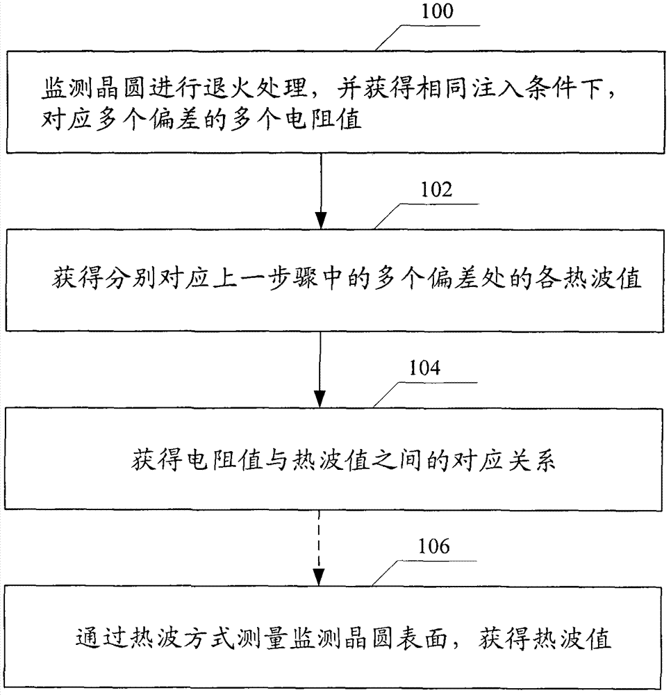
[0013] figure 1 It is a schematic flow chart of the method of the present invention. As shown in the figure, in the process step 100, several monitoring wafers are annealed, and multiple resistance values ​​corresponding to multiple deviations are obtained under the same implantation conditions. The term "same implantation conditions" refers to the same control conditions for ion implantation, such as the same parameters such as implantation d...


PUM


Abstract

The invention provides an ion implantation monitoring method which includes that a thermal wave is adopted to measure the surface of a wafer so as to obtain hot wave value, and according to the relation between pre-determined hot wave value and resistance of the wafer after annealing, the resistance of the wafer is confirmed so as to monitor ion implantation of the wafer. According to the ion implantation monitoring method, monitoring time can be monitored.

Description

technical field [0001] The invention relates to a semiconductor ion implantation process, in particular to the monitoring of the dopant dose of the substrate ion implantation. Background technique [0002] Methods for fabricating metallization semiconductor (MOS) devices are well developed. During the manufacturing process, the silicon substrate is doped with P-type or N-type impurities. During the ion implantation process, it is very important to monitor the ion implantation to ensure that the correct amount of ions are implanted into the silicon substrate. [0003] For the monitoring of ion implantation, the conventional technology is to measure the monitoring wafer by means of annealing, which is achieved by measuring the resistance of the wafer after annealing. In some cases, however, rapid thermal annealing cannot determine the implantation, for example in cases where the injection interruption job record cannot be determined. Contents of the invention [0004] In ...

Claims


Application Information

Patent Timeline
IPC IPC(8): H01L21/66H01J37/244
Inventor 苏小鹏龚榜华郭楠
Owner CSMC TECH FAB2 CO LTD
Why Eureka
Try Eureka