Method for improving polycrystalline silicon furnace tube control wafer monitoring mechanism

A technology of polysilicon and wafers, which is applied in the field of improving the control mechanism of polysilicon furnaces, can solve the problems of increasing the cost of schedule monitoring, increasing the number of particles and film thickness, and reducing the efficiency of schedule monitoring, so as to reduce the number of slices and measurement time, Improve the monitoring mechanism and the effect of consistent deposition rate

Inactive Publication Date: 2014-09-17
SHANGHAI HUALI MICROELECTRONICS CORP
View PDF6 Cites 8 Cited by
  • Summary
  • Abstract
  • Description
  • Claims
  • Application Information

AI Technical Summary

Problems solved by technology

[0007] The above-mentioned patents have the problem of using a large number of tablets for control, and measuring the number of particles and film thickness before and after the process of controlling the film for a long time, which increases the cost of schedule monitoring and reduces the efficiency of schedule monitoring

Method used


Image

  • Method for improving polycrystalline silicon furnace tube control wafer monitoring mechanism
  • Method for improving polycrystalline silicon furnace tube control wafer monitoring mechanism
  • Method for improving polycrystalline silicon furnace tube control wafer monitoring mechanism

Examples


Embodiment Construction

[0031] The present invention will be further described below with reference to the drawings and specific embodiments. Obviously, the described examples are only a part of the examples of the present invention, rather than all examples. Based on the examples summarized in the present invention, all examples obtained by those of ordinary skill in the art without creative work shall fall within the protection scope of the present invention.

[0032] It should be noted that the examples in the present invention and the features in the examples can be freely combined with each other if there is no conflict.

[0033] The present invention is a method for improving the monitoring mechanism of polysilicon furnace management and control slices, which includes the following steps:

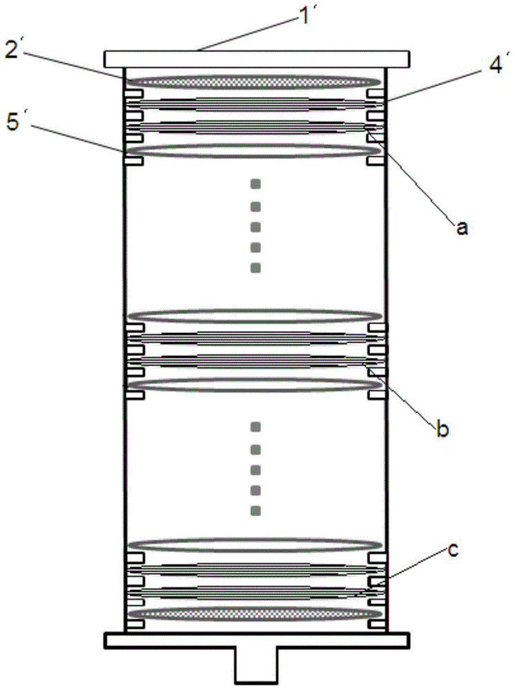
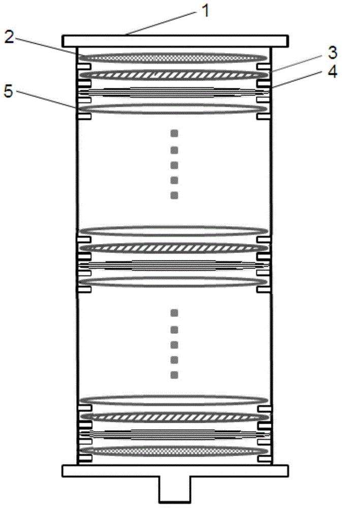
[0034] Step S1, providing a wafer boat, a number of product chips, a number of first baffles, a number of second baffles, and a number of control sheets;

[0035] Step S2: From top to bottom in the wafer boat, a fir...


PUM


Abstract

The invention provides a method for improving a polycrystalline silicon furnace tube control wafer monitoring mechanism and relates to the technical field of semiconductor manufacturing. The method comprises the following steps that three non-product wafer zones are arranged in a wafer boat; zones except for the three non-product wafer zones in the wafer boat are filled with a plurality of product wafers and a plurality of first stopping sheets; the non-product wafer zones are filled with first stopping sheets, second stopping sheets and control wafers; the wafer boat is placed in a furnace tube for a polycrystalline silicon manufacturing technology; the used second stopping sheets are washed and remanufactured; the steps are repeated, wherein each second stopping sheet is formed after silicon nitride and silicon oxide are deposited on a polished section and only silicon oxide is deposited on the control wafers. The polycrystalline silicon deposition speed on the control wafer and the polycrystalline silicon deposition speed on the surfaces of the product wafers are identical in the furnace tube technology process, the number of particles and the thicknesses of films of the product wafers can be effectively and accurately reflected through the control wafers, the number of the control wafers is reduced, the measurement time is shortened, and therefore the cost for schedule monitoring is reduced and the efficiency for schedule monitoring is improved.

Description

Technical field [0001] The invention relates to the technical field of semiconductor manufacturing, in particular to a method for improving the monitoring mechanism of a polysilicon furnace management and control chip. Background technique [0002] In the prior art, the deposition of polysilicon in the semiconductor structure usually adopts a low-pressure chemical vapor deposition vertical furnace tube. In order to ensure the process quality of the furnace tube, in the furnace tube process, the upper, middle, and Two adjacent control plates are placed in the lower position to detect whether the particle number and film thickness of the process product in the furnace tube meet the process standards. The structure is as follows figure 1 As shown, it includes a wafer boat 1', a number of baffles 2', a number of control plates 4', and a number of product wafers 5'. [0003] Among them, for most semiconductor manufacturing processes, before the product wafer 5'enters the polysilicon fur...

Claims


Application Information

Patent Timeline
IPC IPC(8): H01L21/67
CPCH01L22/12H01L22/30
Inventor 吴加奇王智苏俊铭张旭昇
Owner SHANGHAI HUALI MICROELECTRONICS CORP
Why Eureka
Try Eureka