Metal nanowire surface plasma modulator based on grapheme two-dimension material

A surface plasmon, metal nanowire technology, applied in instruments, light guides, optics, etc., can solve problems such as difficulty and few modulation schemes, and achieve the effect of changing light absorption characteristics

Active Publication Date: 2013-05-15
ZHEJIANG UNIV
View PDF2 Cites 16 Cited by
  • Summary
  • Abstract
  • Description
  • Claims
  • Application Information

AI Technical Summary

Problems solved by technology

However, it is difficult for such heavy metals to adjust their electron density, so it is very difficult to modulate surface plasmons, and there are few modulation schemes

Method used


Image

  • Metal nanowire surface plasma modulator based on grapheme two-dimension material
  • Metal nanowire surface plasma modulator based on grapheme two-dimension material
  • Metal nanowire surface plasma modulator based on grapheme two-dimension material

Examples


Embodiment Construction

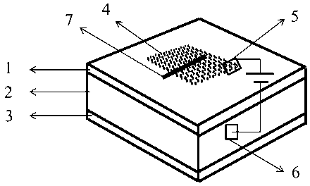
[0012] Such as figure 1 As shown, the metal nanowire surface plasmon modulator based on graphene two-dimensional material of the present invention includes a substrate, graphene 4 and metal nanowire 7, wherein the substrate includes a first silicon dioxide layer 1, a silicon layer 2 and The second silicon dioxide layer 3, the first silicon dioxide layer 1 and the second silicon dioxide layer 3 are grown on the upper and lower surfaces of the silicon layer 2 respectively, and graphene 4 is placed on the first silicon dioxide layer 1, and the graphene 4 is connected to the first electrode 5, the silicon layer 2 is connected to the second electrode 6, one end of the metal nanowire 7 is located on the first silicon dioxide layer 2, and the other end is located on the graphene 4.

[0013] The thickness of the first silicon dioxide layer 2 is 30-300nm, preferably 300nm,

[0014] Graphene 4 is a two-dimensional material of single-layer or double-layer graphene. Graphene 4 is direct...


PUM

PropertyMeasurementUnit
thicknessaaaaaaaaaa
diameteraaaaaaaaaa

Abstract

The invention discloses a metal nanowire surface plasma modulator based on grapheme two-dimension material. The metal nanowire surface plasma modulator based on grapheme two-dimension material includes placing a metal nanowire on the grapheme and triggering the surface plasma of the metal nanowire through a laser. The surface plasma of the metal nanowire interacts with the grapheme material through energy level transition in a transmission process. Fermi level of the grapheme is adjusted, so light absorption characteristic of the grapheme can be greatly changed. Due to increasing or reduction of absorption of surface plasma of the metal nanowire through the grapheme, modulation on surface plasma can be achieved. Due the fact that the grapheme has the advantages of being small in size (monatomic layer), high in carrier speed, adjustable in the Fermi level and the like, the metal nanowire surface plasma modulator based on grapheme two-dimension material expresses huge advantages in absorption and modulation of the surface plasma.

Description

technical field [0001] The invention relates to a micro-nano photonics element, in particular to a metal nanowire surface plasmon modulator based on graphene two-dimensional material. Background technique [0002] Due to the super-diffraction limit ability of surface plasmons, it shows great potential in the research field of micro-nanophotonics, and has attracted extensive attention of researchers in recent years. The ideal materials for surface plasmons are heavy metals, such as gold, silver and so on. However, it is difficult for such heavy metals to adjust their electron density. Therefore, it is very difficult to modulate surface plasmons, and there are few modulation schemes. Graphene materials, which have attracted widespread attention in recent years, have shown great application potential in light and plasmonic modulation due to their fast carrier velocity and easy adjustment of Fermi level. Contents of the invention [0003] The object of the present invention ...

Claims


Application Information

Patent Timeline
Patent Type & Authority Applications(China)
IPC IPC(8): G02B6/122
Inventor 杨青钱浩亮马耀光刘旭
Owner ZHEJIANG UNIV
Why Eureka
Try Eureka