Double-booting method based on single FLASH storage chip

A memory chip, a single technology, applied in the direction of program loading/starting, program control devices, etc., can solve the problems of large size, high cost of embedded systems, and high consumption of system resources, and achieve the effect of solving poor reliability and increasing hardware costs

Inactive Publication Date: 2013-05-22
FENGHUO COMM SCI & TECH CO LTD
View PDF10 Cites 18 Cited by
  • Summary
  • Abstract
  • Description
  • Claims
  • Application Information

AI Technical Summary

Problems solved by technology

[0007] The technical problem to be solved by the present invention is to solve the problems of high cost, large volume and high system resource consumption of the embedded system that adopts dual FLASH memory chip BOOT to start

Method used


Image

  • Double-booting method based on single FLASH storage chip
  • Double-booting method based on single FLASH storage chip
  • Double-booting method based on single FLASH storage chip

Examples


Embodiment Construction

[0048] The present invention will be described in detail below in conjunction with the accompanying drawings.

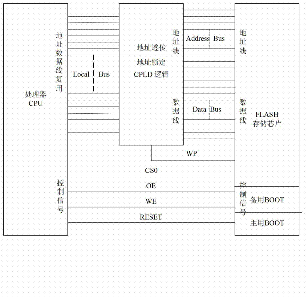
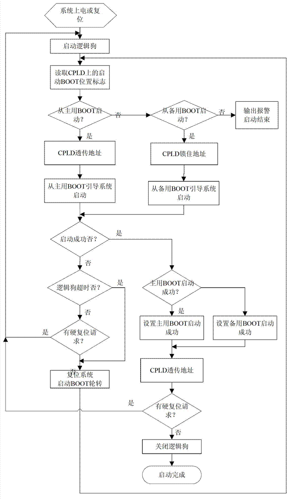
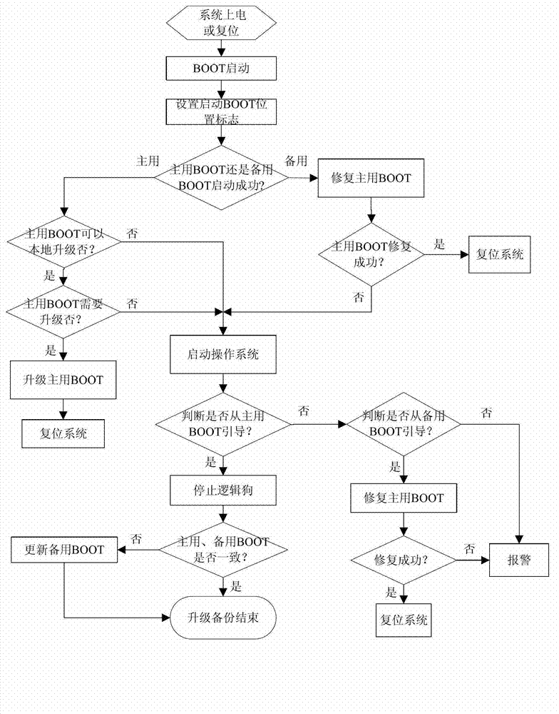
[0049] Such as figure 1 As shown, in the dual-boot implementation method based on a single FLASH memory chip provided by the present invention, the main BOOT and the standby BOOT are respectively stored in different positions of the FLASH memory chip (the general practice is to store them at the end of the FLASH memory chip), The address line of the CPU is connected with the address line of the FLASH memory chip through the CPLD logic module. The CPLD logic module realizes two functions, one is to transparently transmit the CPU address information to the FLASH memory chip, so as to start the system from the main BOOT (by default), and the other is to lock the location of the standby BOOT program in the FLASH memory Corresponding address lines to realize booting from the standby BOOT (when the main BOOT fails to boot and is switched to the standby BOOT). There are t...


PUM


Abstract

The invention discloses a double-booting method based on a single FLASH storage chip. The double-booting method based on the single FLASH storage chip includes the following steps: a master BOOT and a backup BOOT are respectively stored on different positions of the storage chip, and an address wire of a central processing unit (CPU) is connected with an address wire of the storage chip through a complex programmable logic device (CPLD) logic module; a successful booting marker register is arranged on the CPLD logic module, and a corresponding setting is carried out by the successful booting marker register according to whether booting of the master BOOT or the backup BOOT is successful; round robin of the master BOOT and the backup BOOT is carried out by the CPLD logic module according to the state of the successful booting marker register, if booting is carried out by the master BOOT, address information of the CPU is transferred to the storage chip, and system booting is guided from the master BOOT; if booting is carried out by the backup BOOT, the corresponding address wire is locked according to the position of a backup BOOT program in a storer, and the system booting is guided from the backup BOOT. According to the double-booting method based on the single FLASH storage chip, a double-booting function is achieved by adopting only one storage chip, and the problems that a double-FLASH is high in cost, large in size and high in system energy consumption are solved.

Description

technical field [0001] The invention relates to an embedded system, in particular to a dual-boot method based on a single FLASH memory chip. Background technique [0002] In an embedded system, the BOOT program of the device is usually stored at the end of the FLASH memory chip, which is used to start and guide the system when it is powered on. Once the BOOT program data is damaged, the system will not start, which is unacceptable for high reliability systems. [0003] In order to meet the requirements of high-reliability systems for the BOOT startup program, the current industry practice is to use two chip selects to connect two FLASH memory chips. When BOOT on one FLASH memory chip fails, it will automatically switch to the other through chip select. The BOOT of the FLASH memory chip starts the system, so as to enhance the reliability of the system. [0004] However, the above solution needs to use two chip selects and two FLASH memory chips, and each FLASH memory chip s...

Claims


Application Information

Patent Timeline
Patent Type & Authority Applications(China)
IPC IPC(8): G06F9/445
Inventor 刘勇刚胡胜强李传宝陈俊强
Owner FENGHUO COMM SCI & TECH CO LTD
Why Eureka
Try Eureka