Touch control display circuit structure and driving method, array substrate and display device thereof

A circuit structure, touch display technology, applied in static indicators, electrical digital data processing, instruments, etc., can solve the problems of cumbersome process technology and low aperture ratio of finished products, so as to reduce process technology and improve product aperture ratio , the effect of increasing added value

Active Publication Date: 2013-06-05
BEIJING BOE OPTOELECTRONCIS TECH CO LTD
View PDF5 Cites 84 Cited by
  • Summary
  • Abstract
  • Description
  • Claims
  • Application Information

AI Technical Summary

Problems solved by technology

At present, the In cell touch technology has been successfully applied to LCD displays, and the first-line manufacturers in the industry have successfully mass-produced it. However, due to the limitation of patented technology and yield rate, it still cannot completely replace Add on on a large scale in the market. (Add a layer of capacitive film fo

Method used


Image

  • Touch control display circuit structure and driving method, array substrate and display device thereof
  • Touch control display circuit structure and driving method, array substrate and display device thereof
  • Touch control display circuit structure and driving method, array substrate and display device thereof

Examples


Embodiment Construction

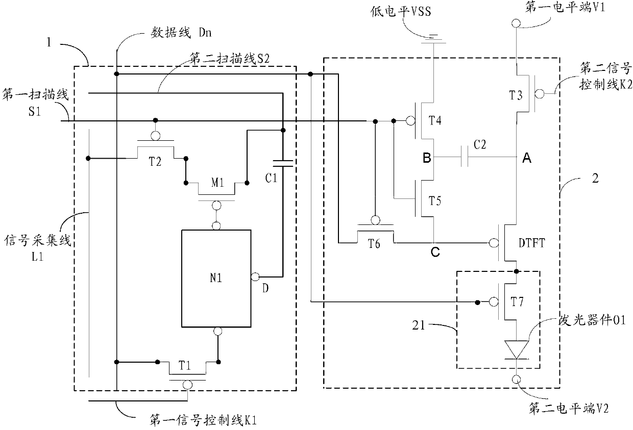
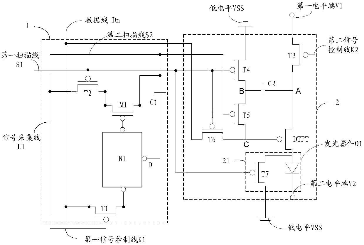
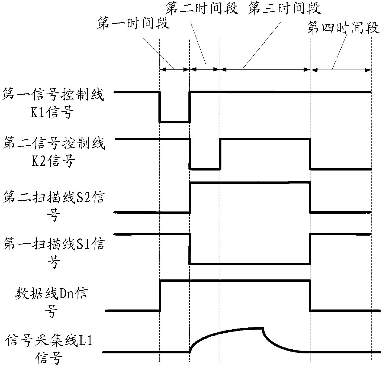
[0060] The following will clearly and completely describe the technical solutions in the embodiments of the present invention with reference to the accompanying drawings in the embodiments of the present invention. Obviously, the described embodiments are only some, not all, embodiments of the present invention. Based on the embodiments of the present invention, all other embodiments obtained by persons of ordinary skill in the art without making creative efforts belong to the protection scope of the present invention.

[0061] The switching transistors, amplifying transistors and driving transistors used in all embodiments of the present invention can be thin film transistors or field effect transistors or other devices with the same characteristics. Since the source and drain electrodes of the switching transistors used here are symmetrical, their Source and drain are interchangeable. In the embodiment of the present invention, in order to distinguish the two poles of the tr...


PUM


Abstract

The invention discloses a touch control display circuit structure and a driving method, an array substrate and a display device thereof, and relates to the field of displayer manufacture. The touch control display circuit structure can reduce manufacturing processes during touch display product producing process, improves aperture opening ratio, and improves product additional value. The touch control display circuit structure comprises a touch control unit, a display unit, a data line, a first scanning line, a second scanning line, a signal collection line, a first signal control line, another one data line, another one first scanning line, another one second scanning line and another one signal control line, wherein the data line, the first scanning line, the second scanning line, the signal collection line and the first signal control line are connected with the touch control unit, and the another one data line, the another one first scanning line, the another one second scanning line and the another one signal control line are connected with the display unit. The touch control display circuit structure is applied to displayer manufacture.

Description

technical field [0001] The present invention relates to the field of display technology, in particular to a touch display circuit structure and a driving method thereof, an array substrate and a display device. Background technique [0002] Organic Light Emitting Diode (Active Matrix / Organic Light Emitting Diode, AMOLED) is one of the hotspots in the field of flat panel display research today. Compared with liquid crystal displays, OLED (Organic Light-Emitting Diode, Organic Light Emitting Diode) has low energy consumption and low production cost. , self-illumination, wide viewing angle and fast response speed, etc. At present, OLED has begun to replace the traditional LCD (Liquid Crystal Display) display screen in the display fields of mobile phones, PDAs (Personal Digital Assistant, handheld computers), digital cameras . At present, the In cell touch technology has been successfully applied to LCD displays, and the first-line manufacturers in the industry have successfull...

Claims


Application Information

Patent Timeline
IPC IPC(8): G06F3/041G09G3/32
CPCG09G3/3233G09G2300/0842G09G2310/0262G06F3/0412
Inventor 杨盛际
Owner BEIJING BOE OPTOELECTRONCIS TECH CO LTD
Why Eureka
Try Eureka