Semiconductor failure detection structure and formation method, method for detecting failure time

A technology for detecting structure and failure time, which is applied in semiconductor/solid-state device testing/measurement, semiconductor devices, semiconductor/solid-state device components, etc. It can solve the problem of low accuracy of electromigration failure detection structure testing and damage to standardized pad structures, etc. problems, to avoid the expansion of the design area

Active Publication Date: 2015-11-25
SEMICON MFG INT (SHANGHAI) CORP
View PDF5 Cites 0 Cited by
  • Summary
  • Abstract
  • Description
  • Claims
  • Application Information

AI Technical Summary

Problems solved by technology

[0008] The problem solved by the present invention is the problem of low test accuracy of the electromigration failure detection structure and ensures that the test accuracy is improved without adding additional design areas and destroying the standardized pad structure

Method used


Image

  • Semiconductor failure detection structure and formation method, method for detecting failure time
  • Semiconductor failure detection structure and formation method, method for detecting failure time
  • Semiconductor failure detection structure and formation method, method for detecting failure time

Examples


Embodiment Construction

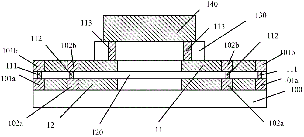
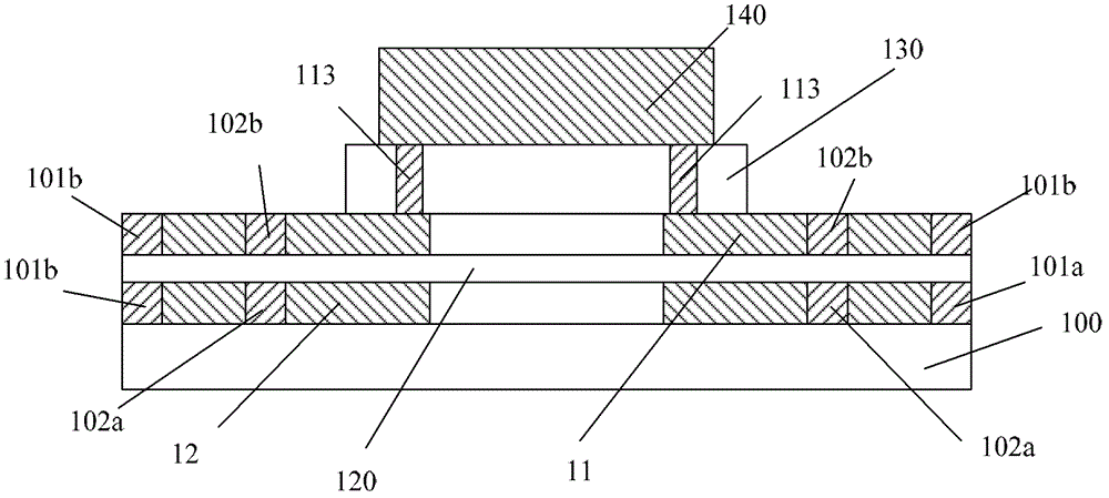
[0054] The inventors found that in the existing electromigration failure detection structure, the accuracy of the test results is reduced due to the parallel connection of each metal layer in the semiconductor device due to the standardized pad structure of the loading point and the test point.

[0055] Specifically, such as figure 1 As shown, the test pad 102 and the test plug 112 form a test pad structure, and the loading pad 101 and the loading plug 111 form a loading pad structure. The pad structure is a standardized structure, which is used to perform various performance tests on each metal layer during the manufacturing process of the semiconductor device, and cannot be removed or damaged in a general process.

[0056] The inventor found through further research that two existing improvements to the electromigration failure detection structure can improve the accuracy of the electromigration test structure.

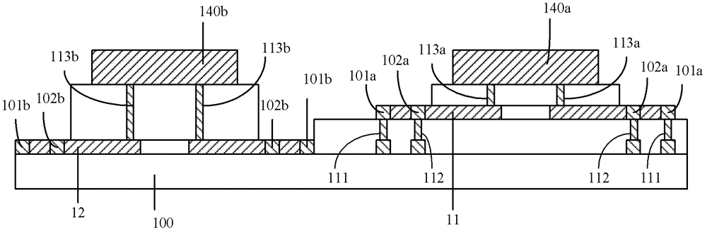
[0057] Specifically, the first improvement method takes fig...


PUM


Abstract

The invention provides a conductor failure detection structure, a forming method and a detection method. The detection structure comprises a substrate, wherein the substrate is provided with a core device area and a peripheral device area. A part of the substrate, located at the core device area, is provided with a first metal layer and a to-be-detected metal layer which are independent, wherein the first metal layer is connected with the to-be-conducted metal layer through a to-be-detected conductive plug. Another part of the substrate, located at the peripheral device area, is provided with a plurality of testing pads and a plurality of loading pads, wherein the testing pads are arranged in an overlapped mode, and the testing pads are connected with the loading pads through a testing conductive plug and a loading conductive plug which penetrate inside a dielectric layer. A pad metal layer is located in the same layer of the to-be-detected metal layer, the pad metal layer is respectively connected with the testing pads and the loading pads through the testing conductive plug and the loading conductive plug, and the pad metal layer is connected with the first metal layer through at least two top-layer conductive plugs. The detection structure can improve accuracy of electromigration detection on the conditions that a standard pad structure is not damaged and the design region area is not enlarged.

Description

technical field [0001] The invention relates to a semiconductor manufacturing process, in particular to a semiconductor failure detection structure and a forming method, and a method for detecting failure time. Background technique [0002] The development requirements of high complexity and high integration of large-scale integrated circuits make semiconductor devices must have higher reliability. However, currently there are many reasons affecting the reliability of semiconductor devices, among which electro-migration (Electro-Migration; EM for short) phenomenon is one of the reasons leading to failure of semiconductor devices. Specifically, electromigration can lead to an open circuit or a short circuit inside a semiconductor device, increasing the leakage of the device and causing it to fail. The cause of electromigration is the movement of metal atoms. When the current density in the metal interconnection line is high, the electrons move from the cathode to the anode a...

Claims


Application Information

Patent Timeline
Patent Type & Authority Patents(China)
IPC IPC(8): H01L23/544H01L21/66
Inventor 陈芳张莉菲
Owner SEMICON MFG INT (SHANGHAI) CORP
Why Eureka
Try Eureka