Amplifier with ultralow direct current (DC) offset at input end and analog/digital (A/D) converter

A DC offset and input technology, applied in analog-to-digital converters, etc., can solve problems such as low temperature drift

Active Publication Date: 2013-06-05
HALO MICROELECTRONICS CO LTD
View PDF4 Cites 14 Cited by
  • Summary
  • Abstract
  • Description
  • Claims
  • Application Information

AI Technical Summary

Problems solved by technology

In many new applications of instrumentation amplifiers, the DC offset at the input of the amplifying component is required to

Method used


Image

  • Amplifier with ultralow direct current (DC) offset at input end and analog/digital (A/D) converter
  • Amplifier with ultralow direct current (DC) offset at input end and analog/digital (A/D) converter
  • Amplifier with ultralow direct current (DC) offset at input end and analog/digital (A/D) converter

Examples


Embodiment 1

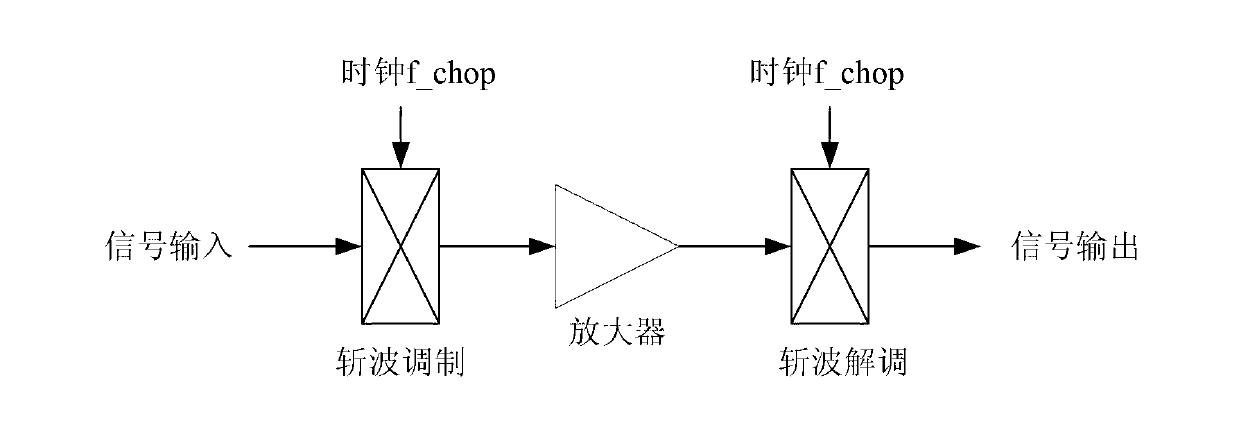
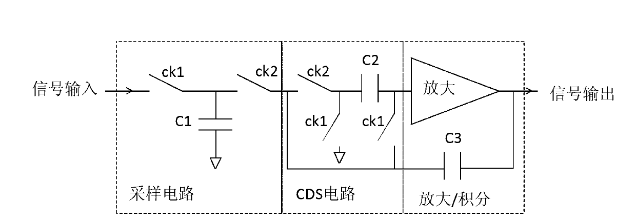
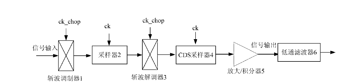
[0038] Such as image 3 , Figure 4 As shown, the amplifier with ultra-low input DC offset includes a chopper modulator 1, a sampler 2, a chopper demodulator 3, a CDS sampler 4, and an amplifier / integrator 5 connected in sequence, where the chopper modulator 1 and Chopper demodulator 3 uses chopping clock signal ck_chop, and sampler 2 and CDS sampler 4 use sampling clock signal ck. The input signal passes through the input chopper modulator 1, sampler 2, chopper demodulator 3 and CDS sampler 4 in sequence, and finally enters the amplifier / integrator 5 to complete the signal amplification and output. In this embodiment, the chopper modulator 1 and the chopper demodulator 3 are respectively arranged at the input end and the output end of the sampler 2 . The large input DC offset of the amplifier / integrator 5 itself is sampled and removed by the CDS sampler 4, while the residual DC offset caused by the non-idealities of the circuit components in the sampler 2, such as switching...

Embodiment 2

[0041] Such as Figure 4 , Figure 5As shown, the amplifier with ultra-low input DC offset includes chopper modulator 1, sampler 2, CDS sampler 4, chopper demodulator 3 and amplifier / integrator 5 connected in sequence, where chopper modulator 1 and Chopper demodulator 3 uses chopping clock signal ck_chop, and sampler 2 and CDS sampler 4 use sampling clock signal ck. The input signal passes through the input chopper modulator 1, sampler 2, CDS sampler 4 and chopper demodulator 3 in sequence, and finally enters the amplifier / integrator 5 to complete the signal amplification and output. In this embodiment, the sampler 2 and the CDS sampler 4 are arranged between the chopper modulator 1 and the chopper demodulator 3, based on the same principle as in embodiment 1, the circuit elements in the sampler 2 and the CDS sampler 4 The remaining DC offset will be modulated to a frequency of 2×ck_chop, generating a high frequency modulation signal.

[0042] The input terminal of the subs...

Embodiment 3

[0044] Such as Figure 4 , Figure 6 As shown, the amplifier with ultra-low input DC offset includes chopper modulator 1, sampler 2, CDS sampler 4, amplifier / integrator 5 and chopper demodulator 3 connected in sequence, where chopper modulator 1 and Chopper demodulator 3 uses chopping clock signal ck_chop, and sampler 2 and CDS sampler 4 use sampling clock signal ck. The input signal is sampled and amplified through the input chopper modulator 1, sampler 2, CDS sampler 4, amplifier / integrator 5 in sequence, and finally output through the chopper demodulator 3. In this embodiment, the sampler 2, the CDS sampler 4, and the amplifier / integrator 5 are all arranged between the chopper modulator 1 and the chopper demodulator 3. Based on the same principle as in Embodiment 1, the sampler 2 , CDS sampler 4 and amplifier / integrator 5 all remaining DC offsets will be modulated to a frequency of 2×ck_chop to generate a high frequency modulation signal.

[0045] Then the output signal ...


PUM


Abstract

The invention relates to an amplifier with ultralow direct current (DC) offset at an input end and an analog/digital (A/D) converter. The amplifier with the ultralow DC offset at the input end comprises a chopped wave modulator, a sampling instrument, a correlated double sampling (CDS) instrument and an amplifying/integration unit which are connected in sequence. A chopped wave demodulator is arranged in a circuit behind the sampling instrument. The chopped wave modulator and the chopped wave demodulator are used for eliminating residual DC offset generated due to imperfection of the CDS instrument and the other circuit components. On the other hand, the CDS instrument can also eliminate residual DC offset of the chopped wave modulator and the chopped wave demodulator. Due to the fact that the chopped wave modulator and the chopped wave demodulator modulate the residual DC offset of the CDS instrument and other circuit components at the clock frequency of 2*ck_chop to generate high-frequency modulating signals, input signals and the modulating signals do not overlap in a frequency domain. Consequently, the modulating signals can be eliminated at a low-pass filter which is connected with an output end of the amplifier with the ultralow DC offset at the input end. Therefore, the purpose of eliminating the residual DC offset of sampling signals is achieved.

Description

technical field [0001] The invention relates to the field of high-precision amplifiers, in particular to an ultra-low input DC offset amplifier and an A / D converter. Background technique [0002] High-precision amplifiers such as instrument amplifiers (Instrument Amplifier) ​​require a very low DC offset (DC offset) at the input. Depending on the application, the input DC offset of the amplifying element is limited to tens to hundreds of microvolts (μV). Wait. If no processing is done at the input end of the amplifying element, the DC offset of the input end of the amplifying element using a bipolar transistor is between 1-3 millivolts (mV), and an insulated gate MOS transistor is used for the amplification of the input stage The dc offset at the component input can be as high as 10 mV, so it is far from adequate. [0003] Commonly used methods to reduce the DC offset at the input of the amplifying element are as follows: [0004] Method 1. Measure and trim the DC offset ...

Claims


Application Information

Patent Timeline
IPC IPC(8): H03M1/12
Inventor 陶海
Owner HALO MICROELECTRONICS CO LTD
Why Eureka
Try Eureka