Optical transport system, optical transmitter device and optical receiver device

An optical transmission and optical transmission technology, applied in the field of optical transmission systems, can solve problems such as unbalanced, excessive signal quality degradation, and achieve the effect of reducing nonlinear interference and improving transmission quality

Inactive Publication Date: 2013-06-05
MITSUBISHI ELECTRIC CORP
View PDF5 Cites 6 Cited by
  • Summary
  • Abstract
  • Description
  • Claims
  • Application Information

AI Technical Summary

Problems solved by technology

In addition, there is a problem that the nonlinear interference generated between Ex-Ey cannot be equaliz

Method used


Image

  • Optical transport system, optical transmitter device and optical receiver device
  • Optical transport system, optical transmitter device and optical receiver device
  • Optical transport system, optical transmitter device and optical receiver device

Examples


Embodiment approach 1

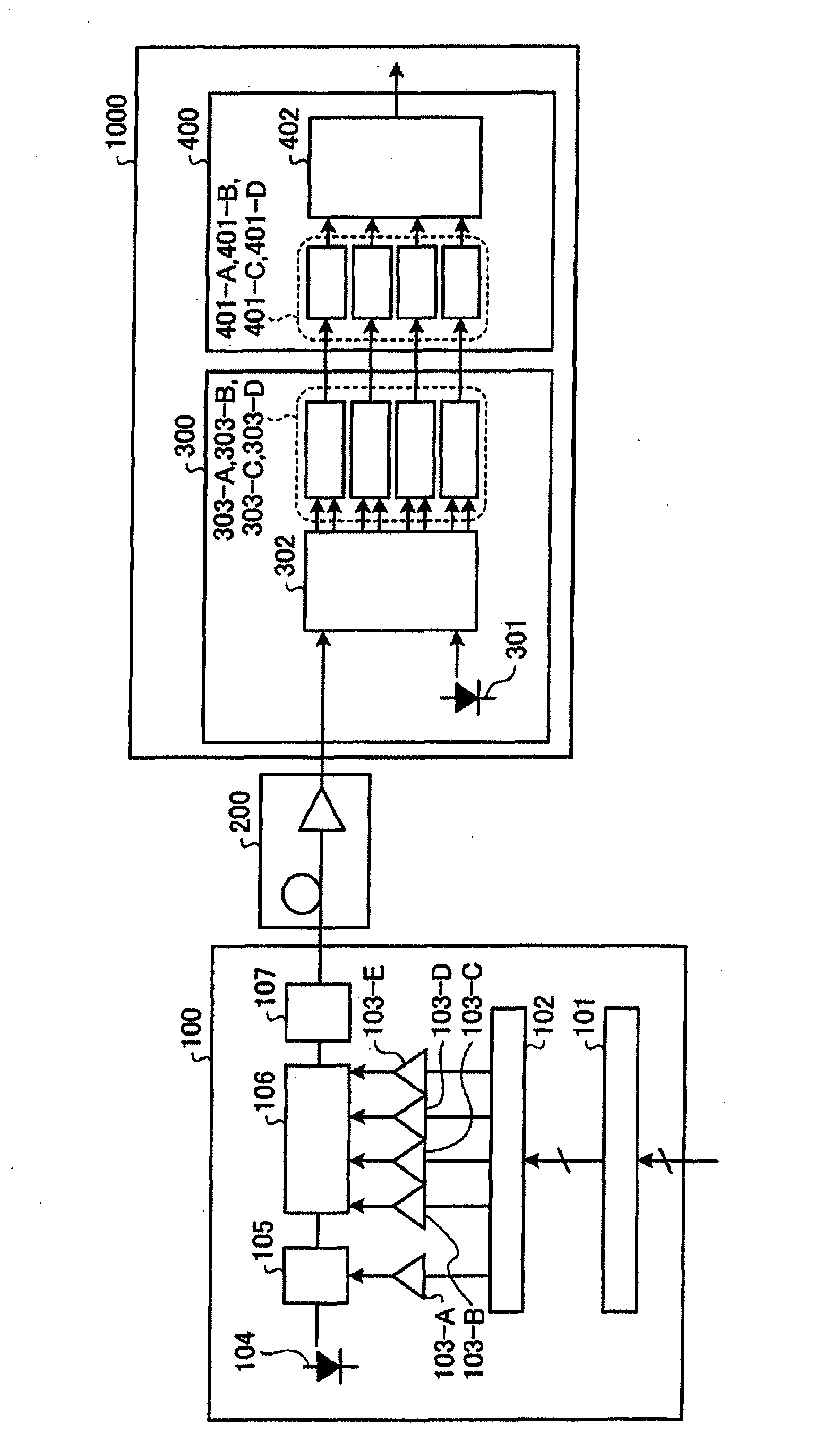
[0040] figure 1 It is a figure which shows the structural example of the optical transmission system of this embodiment. Such as figure 1 As shown, the optical transmission system of this embodiment includes an optical transmission unit (optical transmission device) 100 , an optical transmission unit 200 , and an optical reception device 1000 . The light receiving device 1000 includes a light receiving unit 300 and a received electrical signal processing unit 400 . The same applies to the optical transmission system described in the following embodiments. The optical signal sent from the optical transmission unit 100 reaches the light reception unit 300 via the optical transmission unit 200 . The received optical signal is converted into an electrical signal by the light receiving unit 300 and then electrically processed by the received electrical signal processing unit 400 .

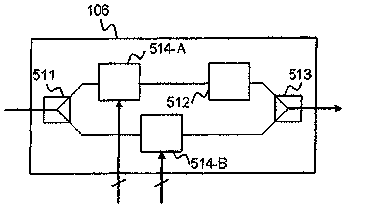
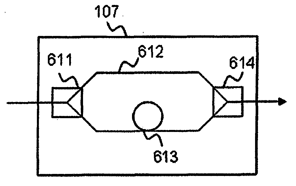
[0041] The optical transmission unit 100 includes a first electrical signal source 101, a seco...

Embodiment approach 2

[0132] In the present embodiment, a CSRZ (Carrier Suppressed Return to Zero) modulation is used for the pulse modulation in the first embodiment described above.

[0133] Figure 13 It is a figure which shows the structural example of the optical transmission system of this embodiment. For those with Embodiment 1 figure 1 The structures with the same functions are attached with the same symbols, and repeated explanations are omitted. The optical transmission system of this embodiment includes an optical transmission unit (optical transmission device) 800 , an optical transmission unit 200 , and an optical reception device 1000 . As shown in the figure, the optical transmission unit 800 includes a first electrical signal source 801, a second electrical signal source 802, electrical amplifiers 803-A, 803-B, 803-C, 803-D, a light source 804, and a Mach-Zehnder modulation device 805. The functions of the light transmitting unit 200 , the light receiving unit 300 , and the rec...


PUM


Abstract

In an optical transport system as laid out in the present invention: at an optical transmitter unit (100), an optical signal is generated such that each polarization component is present so as to be interleaved upon a time axis, wherein the time during which the polarization components are simultaneously present is approximately zero, and the symbol repeating period of the optical signal of each polarization component becomes Ts; at an optical receiver unit (300), after a local oscillator light and the received optical signal are caused to interfere with each other, the optical signal after interference is converted to an electrical signal; and at a received electrical signal processing unit (400), analog/digital conversion of the electrical signal, removal of a delay difference of Ts/2 between each polarization signal component, and adaptive equalization of distortion of other than the delay differences are performed.

Description

technical field [0001] The present invention relates to an optical transmission system using a digital coherent method. Background technique [0002] For large-capacity optical transmission such as 40Gbit / s and 100Gbit / s, overcoming the noise power limit of optical signals and high-density wavelength division multiplexing are issues. As a technology to overcome the limit of optical signal to noise power, binary phase shift modulation (Binary Phase-Shift Keying: BPSK, binary phase shift keying) is known compared to the conventional on-off keying (On-Off Keying: OOK). , 4-value PSK (Quaternary Phase-Shift Keying: QPSK, Quaternary Phase Shift Keying) utilization. In addition, for high-density wavelength division multiplexing, there is known a method of doubling the number of transmission bits per symbol by assigning independent signals to two orthogonal polarization components, such as QPSK. 16-value quadrature amplitude modulation (Quadrature Amplitude Modulation: QAM) is a ...

Claims


Application Information

Patent Timeline
IPC IPC(8): H04B10/532H04B10/61H04J14/00H04J14/06H04B10/50
CPCH04J14/06H04B10/5053H04B10/616H04J14/002H04B10/532
Inventor 吉田刚杉原隆嗣石田和行水落隆司
Owner MITSUBISHI ELECTRIC CORP
Why Eureka
Try Eureka