Gate drive circuit

A gate drive circuit and gate drive technology, applied in instruments, static indicators, etc., can solve problems such as insufficient output capacity of pull-up transistors, achieve the effects of reducing size, improving output capacity, and reducing power consumption

Active Publication Date: 2013-06-12
KUSN INFOVISION OPTOELECTRONICS
View PDF7 Cites 12 Cited by
  • Summary
  • Abstract
  • Description
  • Claims
  • Application Information

AI Technical Summary

Problems solved by technology

[0007] The main technical problem to be solved by the present invention is to provide a gate drive circuit to solve the problem of insufficient output capacit

Method used


Image

  • Gate drive circuit
  • Gate drive circuit
  • Gate drive circuit

Examples


Example Embodiment

[0027] Embodiment one

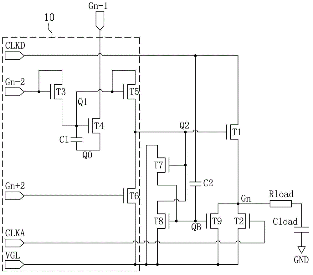
[0028] figure 1 It is a circuit structure diagram of the gate driving unit in Embodiment 1 of the present invention. See figure 1 , the gate driving circuit of this embodiment includes a multi-level gate driving unit, and the gate driving unit is used to output a gate driving signal Gn to respectively drive a corresponding gate line on the display panel. Each stage of the gate driving unit includes a first switching element T1 , a second switching element T2 , a third switching element T3 , a fourth switching element T4 , a fifth switching element T5 and a sixth switching element T6 . Wherein, the first switch element T1 is used as a pull-up switch element, the second switch element T2 is used as a pull-down switch element, and the third switch element T3, the fourth switch element T4, the fifth switch element T5 and the sixth switch element T6 constitute Latch 10.

[0029] Specifically, the first switching element T1 includes a first access end, a ...

Example Embodiment

[0060] Embodiment two

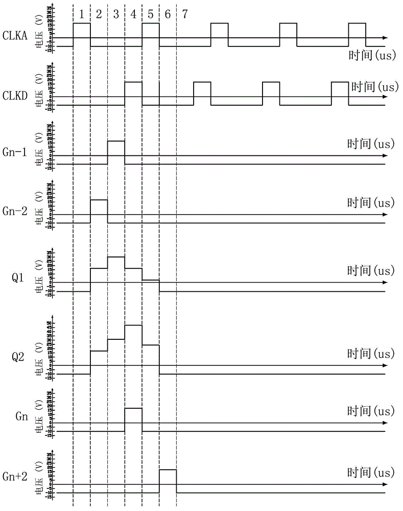
[0061] See Figure 12 , which is a circuit structure diagram of the gate drive circuit in Embodiment 2 of the present invention, and figure 1 The difference is that the figure 1 The seventh switching element T7, the eighth switching element T8, and the tenth switching element T10 are added. The tenth switch element T10 includes a twentieth channel terminal, a tenth control terminal and a nineteenth channel terminal, wherein the twentieth channel terminal is connected to the first channel terminal of the first switch element T1 through the second capacitor C2, and the tenth control terminal The terminal is connected to the output terminal of the gate driving unit, and the nineteenth channel terminal receives the reference low voltage VGL. Depend on figure 2 From the waveform diagram shown in , it can be seen that in this embodiment, the ninth switching element T9 can be turned on at the same time (that is, stage 7), so that the voltage at point Gn i...


PUM


Abstract

The invention provides a gate drive circuit, which comprises multiple stages of gate drive units, wherein each stage of gate drive unit comprises first to sixth switching elements. A latch consists of the third switching element, the fourth switching element, the fifth switching element and the sixth switching element and is used for first-stage pull-up and second-stage pull-up of voltage of control signals output by the latch by receiving the two upper stages of gate drive signals and one upper stage of gate drive signals so as to increase the voltage output by the latch to the first control terminal of the first switching element. According to the gate driving circuit provided by the invention, in a period of time that the gate drive unit outputs the voltage of the gate drive signals, the latch outputs a very high voltage to the control terminal of the first switching element to improve the output capacity of the first switching element, therefore, under the premise of ensuring that the output voltage of gate drive signals is high enough, the size of the first switching element is further reduced, and the power consumption is reduced.

Description

technical field [0001] The invention relates to a driving circuit, in particular to a grid driving circuit suitable for a liquid crystal display device. Background technique [0002] Liquid Crystal Display (LCD) has many advantages such as lightness, lightness, energy saving, and no radiation, so it has gradually replaced the traditional cathode ray tube (CRT) display. Currently, liquid crystal displays are widely used in high-definition digital televisions, desktop computers, personal digital assistants (PDAs), notebook computers, mobile phones, digital cameras and other electronic equipment. [0003] Taking a thin film transistor (Thin Film Transistor, TFT) liquid crystal display device as an example, it includes: a liquid crystal display panel and a driving circuit, wherein the liquid crystal display panel includes a plurality of gate lines and a plurality of data lines, and two adjacent gate lines The line intersects two adjacent data lines to form a pixel unit, and eac...

Claims


Application Information

Patent Timeline
IPC IPC(8): G09G3/36
Inventor 李亚锋李全虎房耸
Owner KUSN INFOVISION OPTOELECTRONICS
Why Eureka
Try Eureka