Super computing system oriented self-gating boundary scan test method and device

A technology of boundary scan and test method, which is applied in the direction of measuring devices, measuring electricity, and measuring electrical variables, etc., can solve problems such as poor flexibility and complicated backplane wiring, and achieve the effects of improving efficiency, improving flexibility, and reducing the number

Active Publication Date: 2014-04-16
NAT UNIV OF DEFENSE TECH
View PDF5 Cites 0 Cited by
  • Summary
  • Abstract
  • Description
  • Claims
  • Application Information

AI Technical Summary

Problems solved by technology

However, the disadvantage of this method is that different boards to be tested can only use the same debugging test command and test data each time, which is less flexible.
In addition, in order to achieve maximum parallelism in the debugging test, the monitoring board can set up a separate JTAG line for all the mainboards to be tested. Although any mainboard in the subrack can be debugged and tested at the same time, this method has the defect of complex wiring on the backplane

Method used


Image

  • Super computing system oriented self-gating boundary scan test method and device
  • Super computing system oriented self-gating boundary scan test method and device
  • Super computing system oriented self-gating boundary scan test method and device

Examples


Embodiment Construction

[0028] The present invention will be further described in detail below in conjunction with the accompanying drawings and specific embodiments.

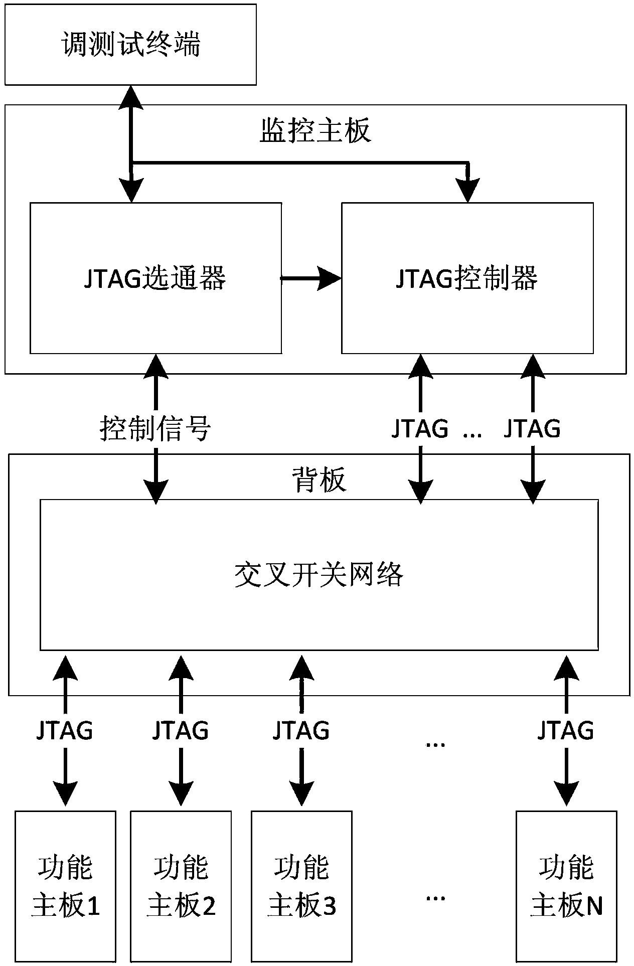
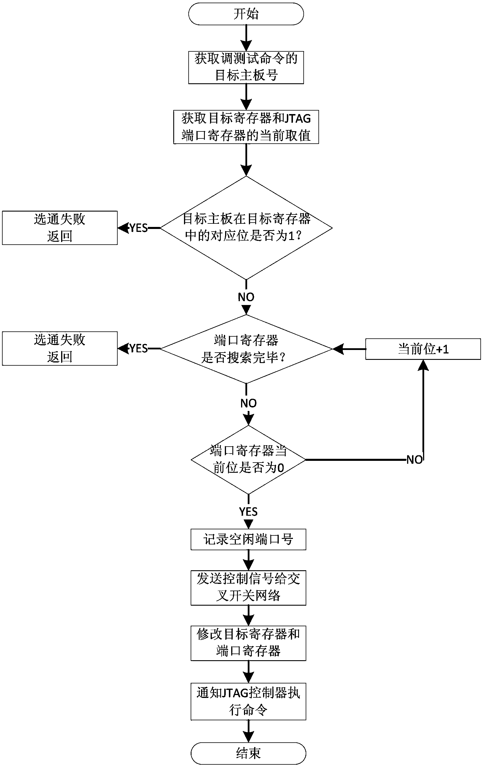
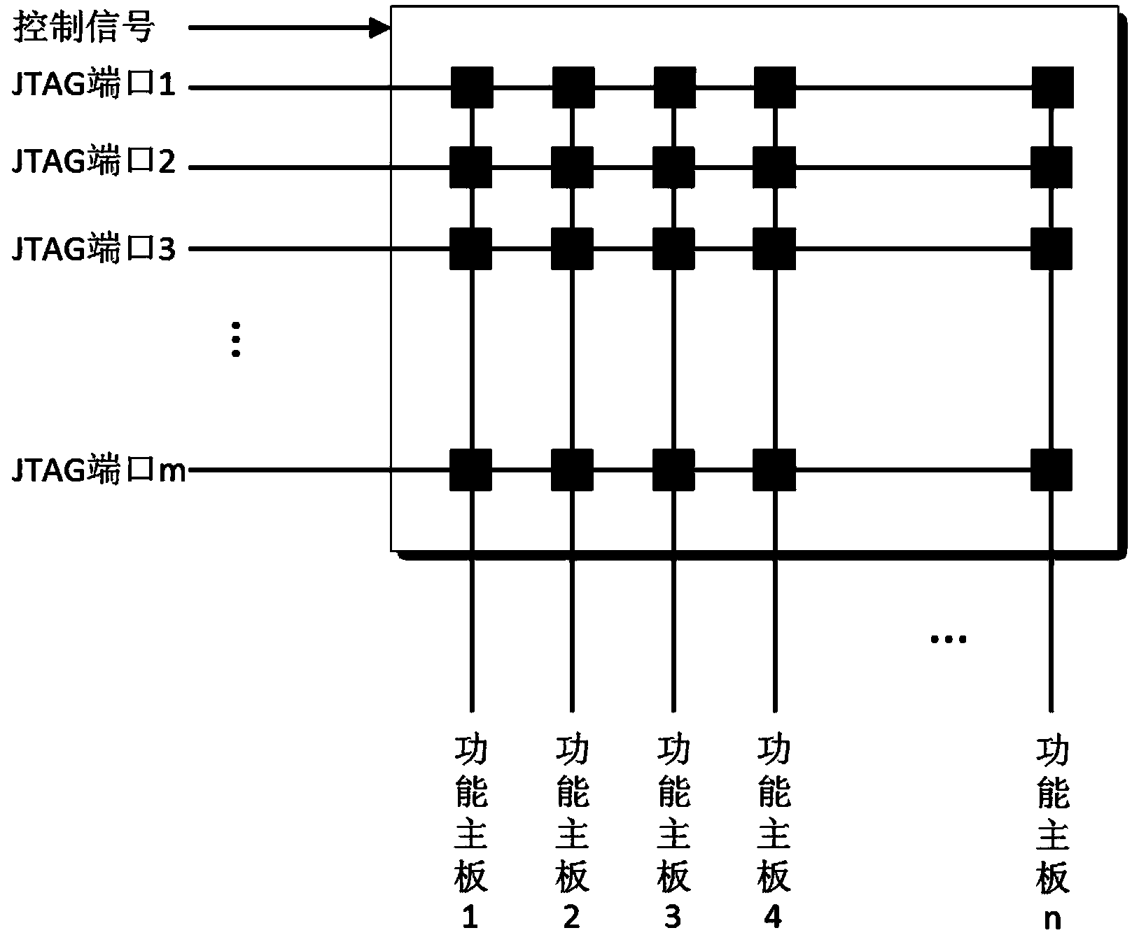
[0029] The supercomputing system-oriented self-selection boundary scan debugging test method of the present invention calculates the optimal tuning test JTAG line according to the input target motherboard number, debugging test command and debugging test concurrency, so as to determine the JTAG output port of the monitoring motherboard and issue control Signal; use the crossbar network on the backplane to receive the control signal of the JTAG strobe, change the on-off of each switch in the crossbar network according to the control signal, complete the strobe and use the gated JTAG output port to execute the debug test command.

[0030] When performing strobing, a certain number of target registers are set according to the number of mainboards to be tested, and if a certain bit is 1, it indicates that the mainboard to be tested corresp...


PUM


Abstract

The invention discloses a super computing system oriented self-gating boundary scan test method and a super computing system oriented self-gating boundary scan test device. The method comprises the following steps of: calculating to obtain the optimum test joint test action group (JTAG) line according to an input target main board number, a test command and test concurrency to determine a JTAG output port of a monitoring main board and send a control signal; and receiving the control signal of a JTAG gate by using a crossbar network on a rear panel, and changing turn-on and turn-off of each switch in the crossbar switch network according to the control signal to finish gating and executing a test command by using the gated JTAG output port. The device comprises a JTAG controller and the JTAG gate which are positioned on the monitoring main board, and a crossbar switch network module positioned on the rear panel. The method and the device have the advantages of simple structure, few rear panel wire, high test flexibility, high test efficiency and balanced JTAG line load.

Description

technical field [0001] The invention mainly relates to the technical field of boundary scan debugging and testing, in particular to a supercomputing system-oriented self-selecting boundary scanning testing method and device. Background technique [0002] The Boundary Scan Test technology uses the additional Boundary Scan Unit and its control logic in the chip pin to realize the debugging and testing function independent of the packaging method, which overcomes the low efficiency, high cost and poor reliability of the traditional "probe" method. question. In 1990, the Institute of Electrical and Electronics Engineering (IEEE) approved the boundary-scan test specification drafted by the Joint Test Action Group, forming the IEEE standard 1149.1, referred to as the JTAG standard. Since the boundary scan technology was proposed, it has been widely used to debug the internal logic of the test chip, the connection between chips and the connection between complex printed boards (PC...

Claims


Application Information

Patent Timeline
Patent Type & Authority Patents(China)
IPC IPC(8): G01R31/3185
Inventor 蒋句平袁远肖立权田宝华李宝峰郑明玲张晓明李小芳邢建英孙言强李琼孙岩李根前
Owner NAT UNIV OF DEFENSE TECH
Why Eureka
Try Eureka