Thin film structure of solar cell absorbing layer and manufacturing method thereof

A technology of solar cells and thin film structures, applied in the direction of final product manufacturing, sustainable manufacturing/processing, circuits, etc., can solve the problems of reduced light absorption range, inability to obtain solar cell absorption layers, etc., to avoid the reduction of absorption range and improve efficiency , the effect of Canon gap width

Inactive Publication Date: 2015-07-29
广东金光伏能源投资有限公司
View PDF5 Cites 0 Cited by
  • Summary
  • Abstract
  • Description
  • Claims
  • Application Information

AI Technical Summary

Problems solved by technology

[0007] Aiming at the deficiencies of the prior art, the object of the present invention is to provide a solar cell absorbing layer thin film structure to solve the problem that the light absorption range of the existing stacked solar cells decreases with the increase of the energy gap width
[0008] In view of the deficiencies in the prior art, the purpose of the present invention is also to provide a method for manufacturing a solar cell absorbing layer thin film structure, which solves the problem that the existing method cannot obtain a solar cell absorbing layer with a real laminated structure

Method used


Image

  • Thin film structure of solar cell absorbing layer and manufacturing method thereof
  • Thin film structure of solar cell absorbing layer and manufacturing method thereof
  • Thin film structure of solar cell absorbing layer and manufacturing method thereof

Examples


Embodiment Construction

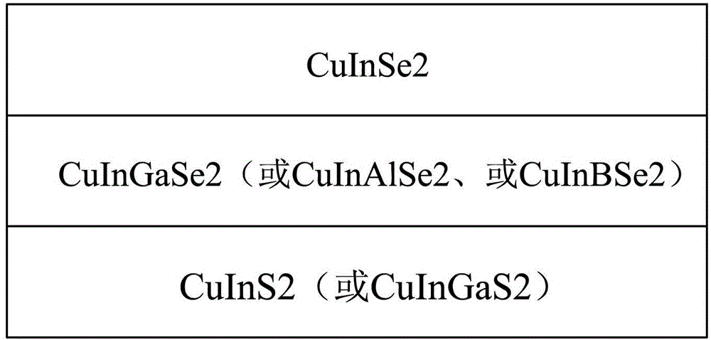
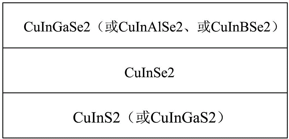
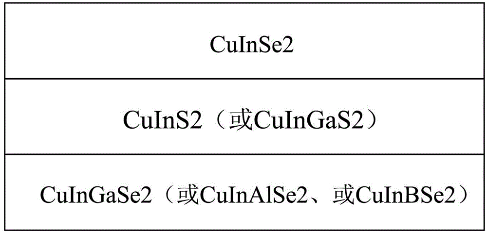
[0032] Hereinafter, the structural characteristics and forming method of the thin film structure of the absorption layer of the CIGS solar cell provided by the present invention will be described with reference to the accompanying drawings.

[0033] The thin film structure of the absorption layer of the copper indium gallium selenide solar cell, such as figure 1 shown, including sequentially stacked CuInSe 2 Thin film layer, CuInGaSe 2 thin film layer (or CuInAlSe 2 Thin film layer, or CuInBSe 2 thin film layer) and CuInS 2 thin film layer (or CuInGaS 2 film layer), as for the buffer, conduction, electrode layer and substrate required to be provided on both sides of the absorbing layer film, they are all the same as the prior art, so they are not drawn in the drawings.

[0034] And the manufacturing method of the absorption layer film structure of the copper indium gallium selenide solar cell comprises the following steps:

[0035] Step 1, preparing the CuInSe 2 Thin fi...


PUM


Abstract

The invention provides a solar cell absorption layer thin film structure and a manufacturing method thereof. The thin film structure comprises three thin film layers arranged in an overlaid mode, wherein one thin film layer is a CuInSe2 thin film layer; one thin film layer is a CuInGaSe2 thin film layer or a CuInAlSe2 thin film layer or a CuInBSe2 thin film layer; and another thin film layer is a CuInS2 thin film layer or a CuInGaS2 thin film layer. The thin film structure can also be manufactured by arbitrary two of the three thin film layers in an overlaid mode. Compared with a GIGS solar cell absorption layer thin film structure with a single layer structure, the provided GIGS solar cell absorption layer thin film structure not only has an excellent energy gap width, but also avoids reduction of the absorption range of light, and greatly improves efficiency of a solar cell for absorbing solar energy.

Description

technical field [0001] The invention relates to a structure and a processing method of an absorption layer of a copper indium gallium selenium solar cell. Background technique [0002] Ordinary copper indium gallium selenide solar cell absorber film has a single-layer structure and only has a single energy gap width, so the solar cell made in this way has a small open circuit voltage and low cell efficiency. [0003] In order to fully absorb the energy of sunlight, some people thought of selecting compound semiconductor materials with different forbidden energy gap widths for stacking to form a high-efficiency tandem solar cell. [0004] In order to manufacture tandem solar cells, the prior art, such as the preparation method provided by the invention patent with the application number CN200910006531.0 and the invention title "Copper Indium Gallium Selenium Solar Cell, Its Absorbing Layer Film and the Preparation Method and Equipment of the Film" , the first step is to depo...

Claims


Application Information

Patent Timeline
Patent Type & Authority Patents(China)
IPC IPC(8): H01L31/0352H01L31/032H01L31/18
CPCY02P70/50
Inventor 谢祥渊李洁
Owner 广东金光伏能源投资有限公司
Why Eureka
Try Eureka