Infrared light and visible light conversion device

A technology of visible light and infrared light, which is applied in the direction of electric solid-state devices, semiconductor devices, semiconductor/solid-state device manufacturing, etc., to achieve the effect of improving conversion efficiency, compact structure and light weight

Inactive Publication Date: 2013-06-26
YUNNAN UNIV
View PDF4 Cites 13 Cited by
  • Summary
  • Abstract
  • Description
  • Claims
  • Application Information

AI Technical Summary

Problems solved by technology

However, the near-infrared detection range of the infrared detection material (TiOPc thin film) is very narrow, only 600nm-900nm, and the light conversion efficiency is low, which limits its application.

Method used


Image

  • Infrared light and visible light conversion device
  • Infrared light and visible light conversion device
  • Infrared light and visible light conversion device

Examples


Embodiment 1

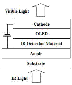
[0028] Embodiment 1: A device for converting infrared light to visible light, which is composed of a substrate 1 , an anode layer 2 , an infrared absorbing material layer 3 , an OLED organic material layer 4 and a cathode layer 5 . in:

[0029] Substrate 1 is glass with better light transmission;

[0030] The anode layer 2 is on the substrate, and the material is indium tin oxide (ITO);

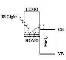
[0031] The infrared absorbing material layer 3 is on the anode layer 2, and the material is MoO 3 CTC formed by doping with CBP at a mass ratio of 3:1, the CTC material has obvious absorption near the wavelength of 840nm;

[0032] OLED organic material layer 4 includes hole injection layer (HIL), hole transport layer (HTL), light emitting layer (EL), electron transport layer (ETL) and electron injection layer (EIL); where:

[0033] The hole injection layer (HIL) uses MoO 3 Material;

[0034] The hole transport layer (HTL) is made of NBP material;

[0035] The light-emitting layer (EL) m...

Embodiment 2

[0040] Embodiment 2: A device for converting infrared light to visible light, which is composed of a substrate 1 , an anode layer 2 , an infrared absorbing material layer 3 , an OLED organic material layer 4 and a cathode layer 5 . in:

[0041] Substrate 1 is glass with better light transmission;

[0042] The anode layer 2 is on the substrate, and the material is indium tin oxide (ITO);

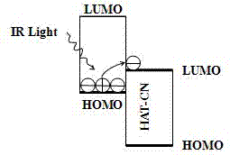
[0043] The infrared absorbing material layer 3 is on the anode layer 2, and the material is a CTC formed by doping HAT-CN and NBP in a mass ratio of 3:7. The CTC material has obvious absorption near a wavelength of 1400nm;

[0044] OLED organic material layer 4 includes hole injection layer (HIL), hole transport layer (HTL), light emitting layer (EL), electron transport layer (ETL) and electron injection layer (EIL); where:

[0045] The hole injection layer (HIL) is made of CuPc material;

[0046] The hole transport layer (HTL) is made of CBP material;

[0047] The luminescent layer (EL) ...

Embodiment 3

[0052] Embodiment 3: A device for converting infrared light to visible light, which is composed of a substrate 1 , an anode layer 2 , an infrared absorbing material layer 3 , an OLED organic material layer 4 and a cathode layer 5 . in:

[0053] Substrate 1 is glass with better light transmission;

[0054] The anode layer 2 is on the substrate, and the material is indium tin oxide (ITO);

[0055] The infrared absorbing material layer 3 is on the anode layer 2, and the material is MoO 3 CTC formed by doping with TCTA at a mass ratio of 3:1, the CTC material has obvious absorption near the wavelength of 1450nm;

[0056] OLED organic material layer 4 includes hole injection layer (HIL), hole transport layer (HTL), light emitting layer (EL), electron transport layer (ETL) and electron injection layer (EIL); where:

[0057] The hole injection layer (HIL) uses MoO 3 Material;

[0058] The hole transport layer (HTL) is made of CBP material;

[0059] The light-emitting layer (EL)...


PUM


Abstract

The invention relates to an infrared light and visible light conversion device, belongs to the field of semiconductor devices and in particular relates to a device which takes a CTC (Charge Transfer Complex) as an infrared detection material, is integrated with an OLED (Organic Light Emitting Diode) and is used for realizing conversion of signal light from an infrared light band to an visible light band. The infrared light and visible light conversion device consists of a substrate, an anode layer, an infrared absorbing material layer, an OLED organic material layer and a cathode layer and is characterized in that the infrared absorbing material is a CTC material which is formed by doping small organic molecules and MoO3 or HAT-CN (Hexaazatriphenylenehexacabonitrile). The infrared light and visible light conversion device disclosed by the invention can be used for realizing the conversion from an infrared band (0.8-1.6mu m) to visible light bands (400nm-440nm, 500-554nm and 620-660nm).

Description

technical field [0001] The invention belongs to the field of semiconductor devices, and in particular relates to a method of using a charge transfer composite material (Charge Transfer Complex, CTC) as an infrared detection material and integrating it with an organic light emitting diode (OLED) to realize signal light from infrared band to visible light Devices for band conversion. Background of the invention [0002] In recent decades, scientists have been exploring a device that can convert infrared radiation that cannot be seen by the human eye into visualization, and integrate it with existing microelectronic devices for applications in photoelectric detection, communications, military, satellites and other fields . In 1995, H. C. Liu first reported the photoelectric-electrical-optic converter integrating QWIP-LED with quantum well infrared detector (QWIP) and LED, which can convert near-infrared light with a wavelength of 1.5 μm into a near-infrared light with a wavel...

Claims


Application Information

Patent Timeline
Patent Type & Authority Applications(China)
IPC IPC(8): H01L27/30H01L27/32H01L51/46
CPCY02E10/549
Inventor 江楠武思平何守杰康滢刘蓝琦王登科刘泰立张涛吕正红
Owner YUNNAN UNIV
Why Eureka
Try Eureka