Inverted organic light emission diode device and manufacturing method thereof

An electroluminescent device, an inverted technology, which is applied in the fields of electro-solid devices, semiconductor/solid-state device manufacturing, electrical components, etc., can solve the problems of high work function, unfavorable electron injection, and difficulty in improving the luminous efficiency of devices.

Inactive Publication Date: 2014-09-17
OCEANS KING LIGHTING SCI&TECH CO LTD +2
View PDF6 Cites 12 Cited by
  • Summary
  • Abstract
  • Description
  • Claims
  • Application Information

AI Technical Summary

Problems solved by technology

[0004] However, for an inverted OLED light-emitting device that emits light from the bottom, a highly transparent electrode is usually required as the cathode. The transmittance of the traditional thin-layer metal is only about 60-70%, and the thin metal film brings challenges to the packaging of the device.
Although the transparent conductive oxide film has high transmittance, its high work function is unfavorable for electron injection, making it difficult to improve the luminous efficiency of the device.

Method used


Image

  • Inverted organic light emission diode device and manufacturing method thereof
  • Inverted organic light emission diode device and manufacturing method thereof

Examples


Embodiment 1

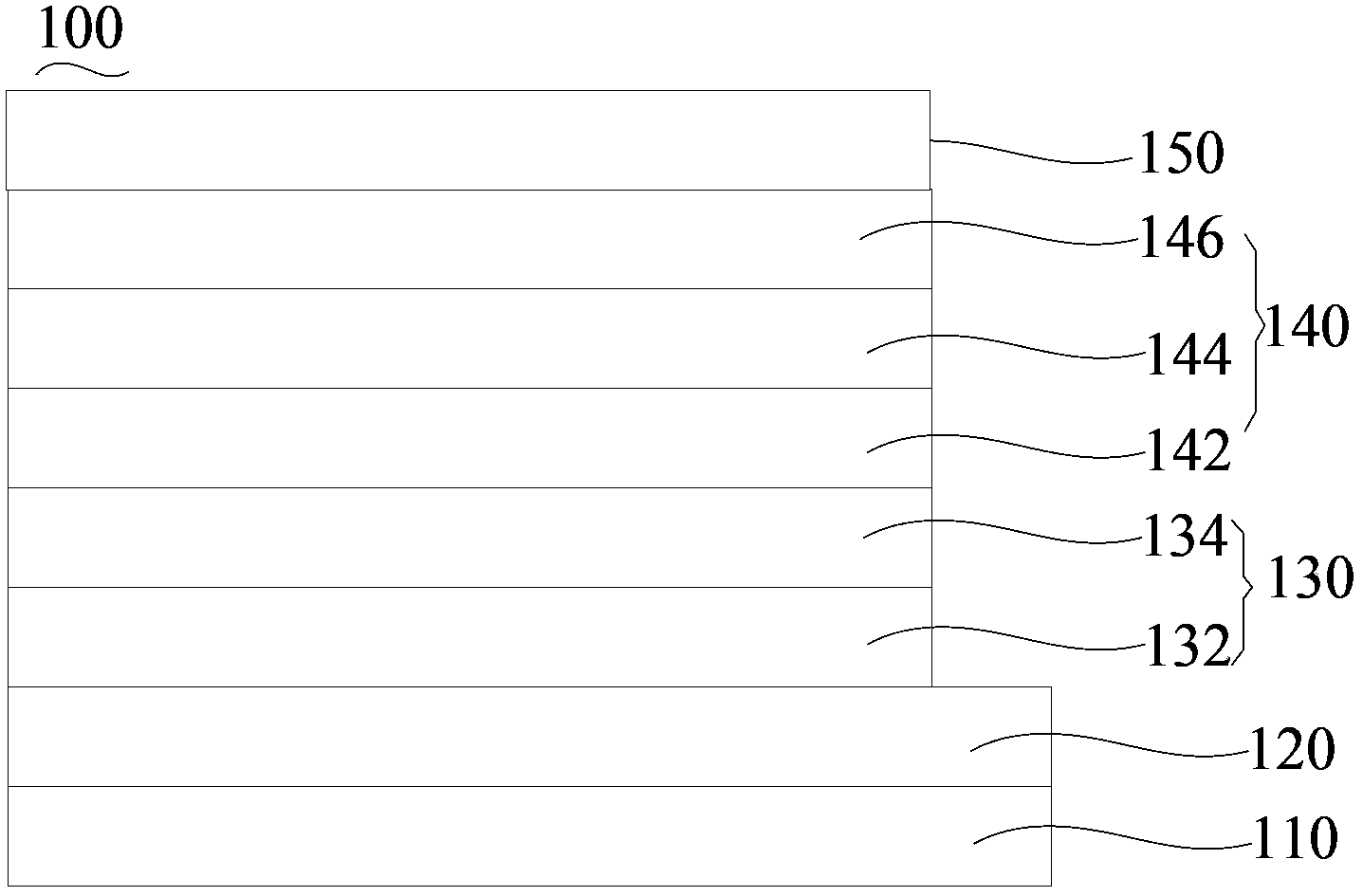
[0048] The structure of the inverted organic electroluminescent device is: glass substrate / ITO(100nm) / CuI:CuPc(5%, 5nm) / F 16 CuPc(4nm) / Bphen(30nm) / DCJTB:Alq 3 (1%, 1nm) / NPB(30nm) / Ag(100nm).

[0049] The fabrication method of the inverted organic electroluminescent device of this embodiment includes the following steps:

[0050] Step 1: Provide a glass substrate, place the substrate in deionized water containing detergent for ultrasonic cleaning, and then use isopropanol and acetone to treat it in ultrasonic waves for 20 minutes, and then dry it with nitrogen.

[0051] Step 2. In a vacuum of 5×10 -4 In Pa's vacuum coating system, a layer of ITO film with a thickness of 100 nm was prepared on the surface of the substrate as the cathode layer by sputtering.

[0052] Step 3. In a vacuum of 5×10 -4 In Pa's vacuum coating system, the p-type layer and n-type layer of the pn junction layer are sequentially prepared on the surface of the cathode layer by thermal evaporation technol...

Embodiment 2

[0057] The structure of the inverted organic electroluminescent device is: glass substrate / AZO(70nm) / ZnI 2 :ZnPc(20%, 15nm) / F 16 ZnPc(10nm) / TPBi(60nm) / Ir(piq) 3 : CBP(8%,12nm) / 2-TNATA(60nm) / Al(70nm).

[0058] The fabrication method of the inverted organic electroluminescent device of this embodiment includes the following steps:

[0059] Step 1: Provide a glass substrate, place the substrate in deionized water containing detergent for ultrasonic cleaning, and then use isopropanol and acetone to treat it in ultrasonic waves for 20 minutes, and then dry it with nitrogen.

[0060] Step 2: In the vacuum coating system, prepare an AZO thin film with a thickness of 70 nm on the surface of the substrate as the cathode layer by sputtering.

[0061] Step 3. In a vacuum of 1×10 -3 In the vacuum coating system of Pa, the p-type layer and n-type layer of the pn junction layer are sequentially prepared on the surface of the cathode layer by thermal evaporation technology, wherein the m...

Embodiment 3

[0066] The structure of the inverted organic electroluminescent device is: glass substrate / GZO(200nm) / SnI 2 :VOPc(1%,4nm) / F 16 CuPc(1nm) / PBD(20nm) / Ir(ppy) 3 : CBP(10%,15nm) / m-MTDATA(20nm) / Au(200nm).

[0067] The fabrication method of the inverted organic electroluminescence device of the present embodiment comprises the following steps:

[0068] Step 1: Provide a glass substrate, place the substrate in deionized water containing detergent for ultrasonic cleaning, and then use isopropanol and acetone to treat it in ultrasonic waves for 20 minutes, and then dry it with nitrogen.

[0069] Step 2: In a vacuum coating system, prepare a GZO thin film with a thickness of 200 nm on the surface of the substrate as a cathode layer by sputtering.

[0070] Step 3. In a vacuum of 1×10 -5 In the vacuum coating system of Pa, the p-type layer and the n-type layer in the pn junction layer are sequentially prepared on the surface of the cathode by thermal evaporation technology, and the mat...


PUM


Abstract

The invention relates to an inverted organic light emission diode device comprising a substrate, a cathode layer, a pn junction layer, an organic light emission function layer, and an anode layer. The layers are successively laminated. The cathode layer is a transparent conductive oxide film; the pn junction layer includes a p type layer approaching the cathode layer and an n type layer arranged on the p type layer; and a light emission layer is arranged in the organic light emission function layer. According to the inverted organic light emission diode device, the transparent conductive oxide film is used for forming the cathode layer and serving as an emergent electrode; and the pn junction layer is designed on the cathode layer and generates charge separation at an exterior electric field, and electrons and holes are respectively transmitted to the organic light emission function layer and the cathode layer from the junctions of the pn junction layer. Therefore, the electrons are injected into the organic light emission function layer, thereby solving a problem of difficult electron injection. The inverted organic light emission diode device prepared based on the design can obtain the high luminous efficiency.

Description

technical field [0001] The invention relates to the technical field of electroluminescence, in particular to an inverted organic electroluminescence device and a manufacturing method thereof. Background technique [0002] Organic Light Emission Diode (hereinafter referred to as OLED) has the characteristics of high brightness, wide range of material selection, low driving voltage, fully cured active light emission, etc., and has the advantages of high definition, wide viewing angle and fast response speed. A display technology and light source with great potential, in line with the development trend of mobile communication and information display in the information age and the requirements of green lighting technology, is the focus of many researchers at home and abroad. [0003] At present, the development of OLED is very rapid. In order to obtain more application fields, researchers have developed OLED light-emitting devices with various structures, such as top-emitting li...

Claims


Application Information

Patent Timeline
Patent Type & Authority Applications(China)
IPC IPC(8): H01L51/52H01L51/54H01L51/56
CPCH10K71/164H10K85/631H10K85/311H10K50/828
Inventor 周明杰王平冯小明陈吉星
Owner OCEANS KING LIGHTING SCI&TECH CO LTD
Why Eureka
Try Eureka