Low-static-power current-mode band-gap reference voltage circuit

A low static power consumption, reference voltage technology, applied in the direction of adjusting electrical variables, control/regulation systems, instruments, etc., can solve problems such as large static power consumption, and achieve the effect of reducing static power consumption

Inactive Publication Date: 2013-07-10
SOUTHEAST UNIV
4 Cites 9 Cited by

AI-Extracted Technical Summary

Problems solved by technology

[0025] Aiming at the problem that the traditional current mode reference voltage has relatively large static power consumption, the present invention provides a current mode bandgap reference voltage circuit with low static power consumption. The grounding resisto...

Abstract

A low-static-power current-mode band-gap reference voltage circuit is based on the basis of a traditional band-gap reference voltage circuit which is provided with two PNP audions Q1 and Q2, three PMOS (positive channel metal oxide semiconductor) transistors M1, M2 and M3, an operational amplifier OP and four resistors R1, R2, R3 and R4. The low-static-power current-mode band-gap reference voltage circuit is characterized by subjecting the traditional band-gap reference voltage circuit to improvements which comprise removing R1 and R3 and additionally and respectively arranging two resistors R5 and R6 between the non-inverting input end of the operational amplifier OP and the drain electrode of the PMOS transistor M3 and between the inverting input end of the operational amplifier OP and the drain electrode of the PMOS transistor M3, wherein the resistance value of the R5 is equal to that of R6. Under the conditions of the same power voltage and the same bias currents of the audions Q1 and Q2, the total static power of the low-static-power current-mode band-gap reference voltage circuit is 70% lower than that of the traditional band-gap reference voltage circuit when the output reference voltage is 1 volt.

Application Domain

Electric variable regulation

Technology Topic

Oxide semiconductorBand gap +11

Image

  • Low-static-power current-mode band-gap reference voltage circuit
  • Low-static-power current-mode band-gap reference voltage circuit
  • Low-static-power current-mode band-gap reference voltage circuit

Examples

  • Experimental program(1)

Example Embodiment

[0033] The principles and features of the present invention will be described below with reference to the accompanying drawings. The examples cited are only used to explain the present invention, and are not used to limit the scope of the present invention.
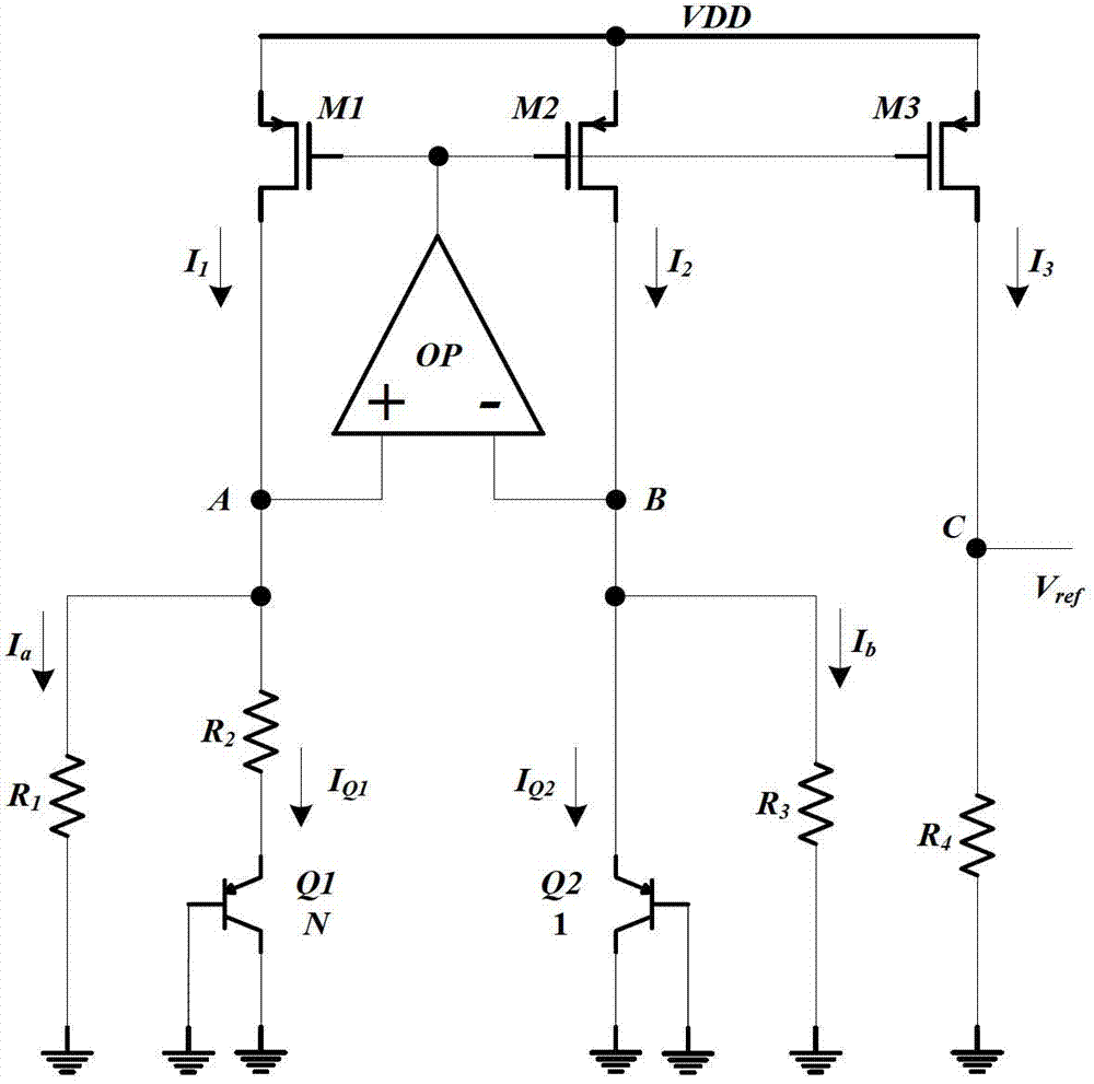
[0034] See figure 2 , The current mode bandgap reference voltage circuit with low static power consumption of the present invention is based on the traditional bandgap reference voltage circuit, including PNP transistors Q1 and Q2, PMOS transistors M1, M2 and M3, operational amplifier OP, resistor R 1 , R 2 , R 3 , R 4; The base and collector of PNP transistors Q1 and Q2 are grounded, and the emitter of PNP transistor Q1 passes through a resistor R 2 With the non-inverting input terminal of the operational amplifier OP, the drain of the PMOS tube M1, and the resistance R 1 Connect one end, resistance R 1 The other end is grounded, the emitter of the PNP transistor Q2 and the inverting input end of the operational amplifier OP, the drain of the PMOS transistor M2, and the resistance R 3 Connect one end, resistance R 3 The other end is grounded, the output end of the operational amplifier OP is connected to the gates of the PMOS transistors M1, M2 and M3, and the drain of the PMOS transistor M3 passes through the resistor R 4 Ground, the source and substrate of the PMOS transistors M1, M2, and M3 are all connected to the power supply voltage VDD, and the drain of the PMOS transistor M3 outputs the reference voltage V ref;
[0035] It is characterized in that the above-mentioned traditional bandgap reference voltage circuit is improved, and the resistance R is removed. 1 , R 3 , A resistor R is added between the non-inverting input terminal of the operational amplifier OP and the inverting input terminal of the operational amplifier OP and the drain of the PMOS tube M3. 5 And R 6. The resistance R 5 =R 6.
[0036] The working principle of the present invention is:
[0037] PMOS transistors M1, M2 and M3 with the same aspect ratio constitute a current mirror of equal proportion, namely I 1 =I 2 =I 3. The operational operational amplifier OP works in deep negative feedback to make the voltages of the nodes A and B of the same direction input terminal and the reverse input terminal equal, in order to ensure I Q1 =I Q2 , Resistance R 5 With R 6 Must take the same resistance, then
[0038] I a = I b = V BE 2 - V ref R 5 = V BE 2 - V ref R 6 (Formula 12)
[0039] Since the base-emitter voltage of the transistor V BE Is the CTAT voltage, then the resistor R 5 Current I a And flow through resistor R 6 Current I b All are CTAT currents. ΔV BE Through resistance R 2 Get a PTAT current I Q1 ,also
[0040] I 3 = I 2 = I 1 = I Q 1 + I a = ΔV BE R 2 + V BE 2 - V ref R 5 = V T ln N R 2 + V BE 2 - V ref R 5 (Formula 13)
[0041] Flow through resistance R 4 Current I 4 The size is:
[0042] I 4 = I 3 + I a + I b = I Q 1 + 2 I a + I b = V T ln N R 2 + 3 ( V BE 2 - V ref R 5 ) (Formula 14)
[0043] So the output reference voltage is:
[0044] V ref = I 4 X R 4 = [ V T ln N R 2 + 3 ( V BE 2 - V ref R 5 ) ] X R 4 (Formula 15)
[0045] After finishing V ref The expression is:
[0046] V ref = R 5 R 5 + 3 R 4 ( V T ln N R 2 + 3 V BE 2 R 5 ) X R 4 (Formula 16)
[0047] When V BE2 ≈750mV, take N=8, V T =26mV, hour, make The reference voltage V with approximately zero temperature coefficient can be obtained ref. Obviously V ref The size can be adjusted by the resistance R 2 , R 4 , R 5 And R 6 Adjust the value arbitrarily.
[0048] When the saturation current I of the PNP transistor Q2 S0 When ≈1fA, it can be obtained by formula 15 Get I from formula 1 Q1 =I Q2 ≈3.37mA, then
[0049] R 2 = V T ln N I Q 2 ≈ 16 Ω , R 5 = 16 X 24.9 = 398.4 Ω (Formula 17)
[0050] Assuming the required reference voltage V ref =1V, R can be obtained by formula 15 4 ≈672.5Ω, if the power supply voltage VDD is 1.5V, the current drawn by the current mirror from the power supply is:
[0051] I 3 = I 2 = I 1 = V T ln N R 2 + V BE 2 - V ref R 5 = 2.75 mA (Formula 18)
[0052] Then the total static power consumption P consumed by the circuit is:
[0053] P=3×I 3 ×VDD=12.375mW (Formula 19)
[0054] It can be seen from the above formula that the new current mode reference circuit proposed by the present invention, under the condition that the power supply voltage and the bias current of the PNP transistors Q1 and Q2 are the same, the total static power consumption when the output reference voltage is 1V is lower than that of the traditional structure By about 70%.

PUM

no PUM

Description & Claims & Application Information

We can also present the details of the Description, Claims and Application information to help users get a comprehensive understanding of the technical details of the patent, such as background art, summary of invention, brief description of drawings, description of embodiments, and other original content. On the other hand, users can also determine the specific scope of protection of the technology through the list of claims; as well as understand the changes in the life cycle of the technology with the presentation of the patent timeline. Login to view more.

Similar technology patents

Gallium nitride power device gate driving circuit

PendingCN113114194AReduce static power consumptionImprove floating ground negative pressure capability
Owner:国硅集成电路技术(无锡)有限公司

Voltage comparator

ActiveCN104158516AReduce static power consumptionLess power consumption branch
Owner:SHENZHEN GOODIX TECH CO LTD

Voltage regulator and electronic device

InactiveCN108733115AReduce static power consumptionMeet the needs of low-power applications
Owner:SEMICON MFG INT (SHANGHAI) CORP +1

Electric control circuit apparatus for relay

InactiveCN101226854AReduce static power consumptionSmall quiescent current
Owner:西蒙电子商务(中国)有限公司

Dynamic energy-saving chip of LED display screen and connecting structure

PendingCN111369937AReduce static power consumptionReduce standby power consumption
Owner:SHENZHEN FM ELECTRONICS GRP CO LTD

Classification and recommendation of technical efficacy words

  • Reduce static power consumption

Voltage comparator

ActiveCN104158516AReduce static power consumptionLess power consumption branch
Owner:SHENZHEN GOODIX TECH CO LTD

Voltage regulator and electronic device

InactiveCN108733115AReduce static power consumptionMeet the needs of low-power applications
Owner:SEMICON MFG INT (SHANGHAI) CORP +1

Dynamic energy-saving chip of LED display screen and connecting structure

PendingCN111369937AReduce static power consumptionReduce standby power consumption
Owner:SHENZHEN FM ELECTRONICS GRP CO LTD

Electric control circuit apparatus for relay

InactiveCN101226854AReduce static power consumptionSmall quiescent current
Owner:西蒙电子商务(中国)有限公司

Gallium nitride power device gate driving circuit

PendingCN113114194AReduce static power consumptionImprove floating ground negative pressure capability
Owner:国硅集成电路技术(无锡)有限公司
Why Eureka
Try Eureka