
Classified power saving circuit and method for dram

A circuit and management circuit technology, applied in the direction of information storage, static memory, digital memory information, etc., can solve problems such as failure, short effective width of data information, unstable reading command data sampling, etc., to improve stability and reduce transient State power consumption, the effect of improving practicality

Active Publication Date: 2017-04-19
XI AN UNIIC SEMICON CO LTD
View PDF5 Cites 0 Cited by
  • Summary
  • Abstract
  • Description
  • Claims
  • Application Information

AI Technical Summary

Problems solved by technology

This kind of operation can bring great power saving effect, so the DRAM industry has continued this kind of control. However, as the speed of DRAM becomes faster and faster, sudden read commands often cause huge transients to the internal and external power supply systems of the chip. Consumption, so that the effective width of the data information generated by the read command is too short, resulting in unstable or even complete failure of the sampling of the read command data

Method used


Image

  • Classified power saving circuit and method for dram
  • Classified power saving circuit and method for dram
  • Classified power saving circuit and method for dram

Examples


Embodiment Construction

[0023] The present invention proposes a DRAM power-saving mode that can reduce transient consumption. The specific method is as follows:

[0024] Normal read command sequence:

[0025] 1. The DRAM is in the stage of power-on completion and is in the state of waiting for instructions. The circuit will make the chip read-related circuits in a fully closed state.

[0026] 2. Activate the word line of the DRAM. The circuit will make the circuit related to the chip read in a half-open state.

[0027] 3. Activate the bit line of the DRAM and send the read command. The circuit will make the chip read related circuit fully open.

[0028] 4. Wait for the read data to be transmitted. The circuit will make the circuit related to the chip read in a half-open state.

[0029] 5. Precharge brings the DRAM back into standby mode. The way will make the chip read-related circuits in a fully closed state.

[0030] Read command sequence 1 including power saving command:

[0031] 1. The ...


PUM


Abstract

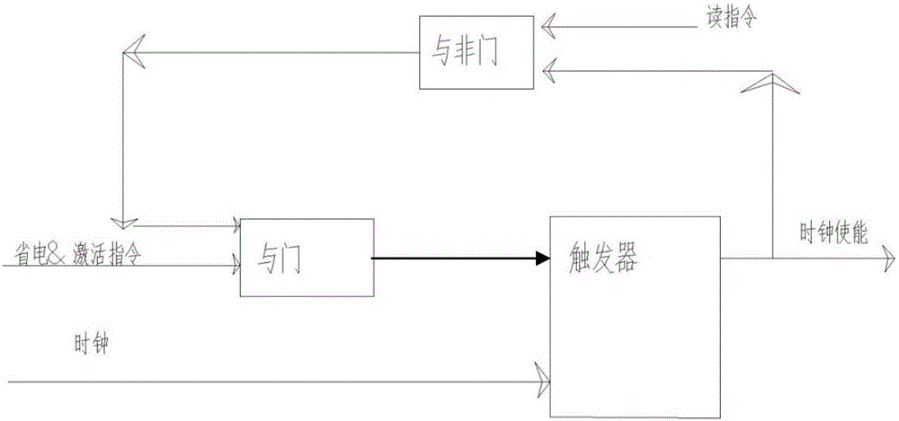
The invention relates to a grading power saving circuit and method used for a DRAM (Dynamic Random Access Memory). The grading power saving circuit comprises a receiver, a DLL (Dynamic Link Library) manager, a delay phase locker DLL, a clock tree circuit and an off-line driver OCD, which are connected in sequence, wherein an internal clock management circuit is arranged between the delay phase locker DLL and the clock tree circuit, and the internal clock management circuit comprises an NAND gate, an AND gate and a trigger, which are connected in sequence. The grading power saving circuit and method used for the DRAM, which are provided by the invention, can enhance the stability and the practicability.

Description

technical field [0001] The invention relates to a hierarchical power saving circuit and method for DRAM. Background technique [0002] In order to meet the power-saving requirements of the JEDEC standard, existing DRAM products often turn on all clocks and corresponding modules inside the chip only when responding to read commands. This kind of operation can bring great power saving effect, so the DRAM industry has continued this kind of control. However, as the speed of DRAM becomes faster and faster, sudden read commands often cause huge transients to the internal and external power supply systems of the chip. consumption, so that the effective width of the data information generated by the read command is too short, resulting in unstable or even complete failure of the sampling of the read command data. Contents of the invention [0003] In order to solve the technical problems in the background art, the present invention proposes a hierarchical power saving method for...

Claims


Application Information

Patent Timeline
Patent Type & Authority Patents(China)
IPC IPC(8): G11C11/4063
Inventor 亚历山大王嵩
Owner XI AN UNIIC SEMICON CO LTD
Learn More