Enhancement type Flash chip, encapsulating method and instruction execution method

An enhanced, chip technology, applied in concurrent instruction execution, machine execution devices, circuits, etc., which can solve the problems of high design cost, long design cycle, and unexpandable Flash capacity.

Active Publication Date: 2013-07-24
GIGADEVICE SEMICON (BEIJING) INC
View PDF5 Cites 6 Cited by
  • Summary
  • Abstract
  • Description
  • Claims
  • Application Information

AI Technical Summary

Problems solved by technology

[0008] The present invention provides an enhanced Flash chip, a packaging method and an instruction execution method to s

Method used


Image

  • Enhancement type Flash chip, encapsulating method and instruction execution method
  • Enhancement type Flash chip, encapsulating method and instruction execution method
  • Enhancement type Flash chip, encapsulating method and instruction execution method

Examples


Embodiment 1

[0077] Embodiment 1 of the present invention proposes an enhanced Flash chip, which may include: multiple FLASHs packaged together and a response protection monotonic counter RPMC.

[0078] In the embodiment of the present invention, each FLASH and RPMC may be independent chips. FLASH can choose different capacities and different processes according to actual needs. The FLASH can reuse the designed FLASH chip, so it does not need to be redesigned, which greatly reduces the development cycle; RPMC has the function of responding to protect the monotonic counting, and can also be used alone.

[0079] In the enhanced Flash chip with RPMC function proposed by the embodiment of the present invention, each FLASH and the RPMC may include their own independent controllers. For commands sent from the outside, each FLASH and RPMC will control each FLASH and RPMC to receive and decode them respectively through their own independent controllers, and perform corresponding operations when t...

Embodiment 2

[0096] In the following, the enhanced Flash chip will be introduced in detail through Embodiment 2 of the present invention.

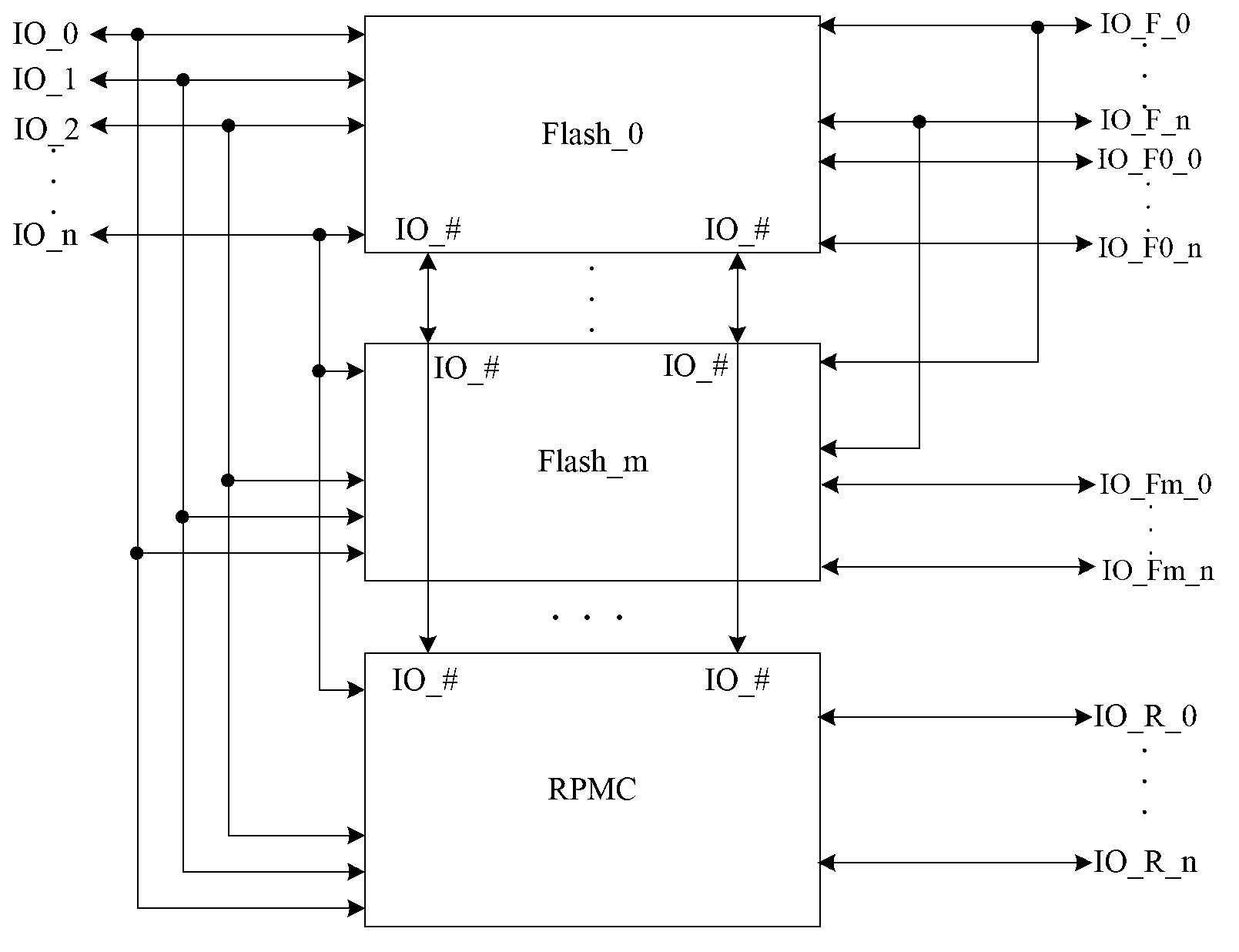
[0097] refer to figure 1 , which shows a schematic diagram of logical connections of an enhanced Flash chip according to Embodiment 2 of the present invention.

[0098] From figure 1 It can be seen that the enhanced Flash chip described in the embodiment of the present invention may include a plurality of FLASH and RPMC packaged together.

[0099] Among them, both FLASH and RPMC include multiple pins, and the same IO pins in RPMC and each FLASH can be connected to the same set of external shared pins, and the commands sent externally will be received by RPMC and each FLASH at the same time. RPMC and each FLASH can respond accordingly.

[0100] FLASH and RPMC also include internal IO pins, internal IO pins of FLASH and internal IO pins of RPMC, and internal IO pin interconnections between different FLASH; RPMC and FLASH will also have their own indep...

Embodiment 3

[0184] Next, the specific packaging method of the above chip will be introduced through the third embodiment of the present invention.

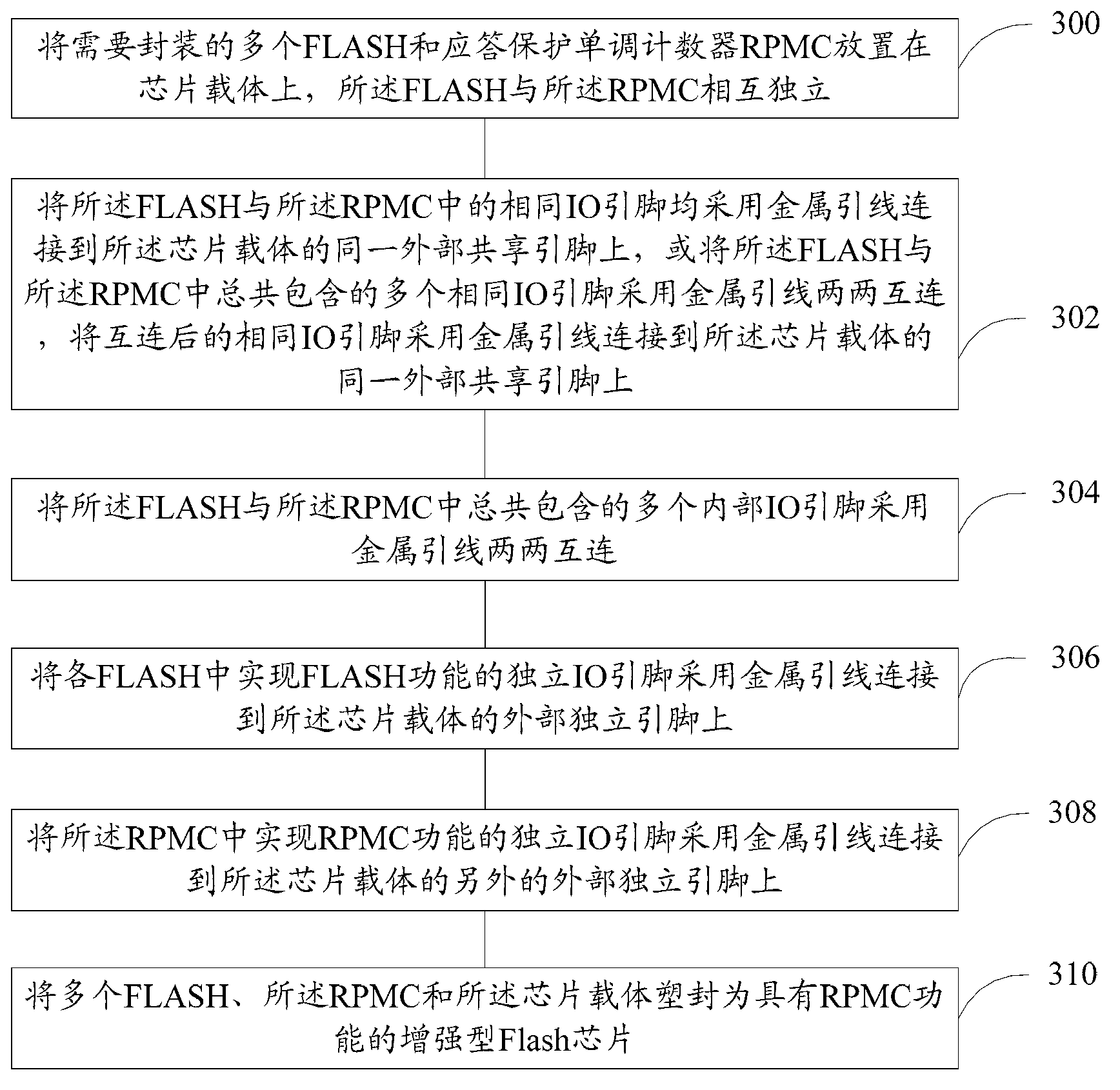
[0185] refer to image 3 , which shows a flowchart of a packaging method described in Embodiment 3 of the present invention, the packaging method may include:

[0186] Step 300, placing multiple FLASHs to be packaged and the response protection monotonic counter RPMC on the chip carrier, the FLASH and the RPMC are independent of each other.

[0187] In the embodiment of the present invention, a plurality of FLASH and RPMC are packaged together to obtain an enhanced Flash chip with RPMC function, and the FLASH and the RPMC in the chip are independent of each other.

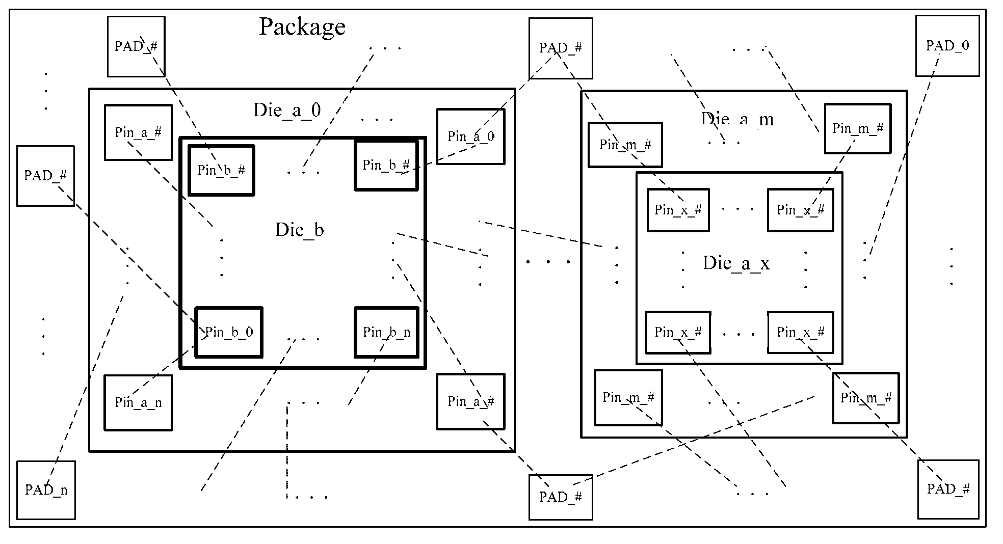
[0188] First, the FLASH and RPMC that need to be packaged can be placed on the chip carrier, and the chip carrier described in the embodiment of the present invention can correspond to figure 2 in the Package.

[0189] Preferably, this step 300 may include: placing a plurality...


PUM


Abstract

The invention provides an enhancement type Flash chip, an encapsulating method and an instruction execution method. The enhancement type Flash chip comprises a plurality of FLASHs encapsulated together and an RPMC (Replay Protection Monotonic Counter), wherein each FLASH and the PRMC respectively comprises respective independent controller, the same IO pin and internal IO pin; the same IO pins in the FLASHs and the PRMC are connected with the same external sharing pin of the chip, or the FLASH and the PRMC comprise a plurality of same IO pins together which are connected with each other and are connected with the same external sharing pin of the chip; and the FLASH and the PRMC comprise a plurality of internal IO pins connected with each other. The problems of nonexpendable Flash volume, high complexity of chip design, long design period and high design cost can be solved.

Description

technical field [0001] The invention relates to the field of chip technology, in particular to an enhanced Flash chip, a packaging method and an instruction execution method. Background technique [0002] The enhanced FLASH with Replay Protection Monotonic Counter (RPMC) is the basic input-output system (Basic Input-Output System, BIOS) chip that Intel will mainly promote. It includes a large-capacity Flash chip and RPMC circuit. Among them, the Flash chip is used to store the code and data of the CPU BIOS, with a capacity of 8M, 16M, 32M, 64M, 128M, 256M or higher; the RPMC circuit is used to protect the confidentiality and integrity of read and write data. The RPMC circuit and its integrated Flash chip constitute the hardware platform of the BIOS in the PC system. [0003] Present RPMC chip integrates high-capacity Flash chip and RPMC circuit on a chip (die), and RPMC circuit and Flash chip are designed together, and this RPMC chip has the following disadvantages: [000...

Claims


Application Information

Patent Timeline
IPC IPC(8): H01L25/18H01L23/528H01L21/60G06F9/38
CPCH01L2224/05554H01L2224/48145H01L2224/49113H01L2224/49171H01L2924/00012
Inventor 胡洪舒清明张赛张建军刘江潘荣华
Owner GIGADEVICE SEMICON (BEIJING) INC
Why Eureka
Try Eureka