Dislocation SMT for FinFET device

A device and dislocation technology, applied in semiconductor devices, semiconductor/solid-state device manufacturing, electrical components, etc., can solve the problem of unusable non-planar devices

Active Publication Date: 2013-08-14
TAIWAN SEMICON MFG CO LTD
View PDF4 Cites 36 Cited by
  • Summary
  • Abstract
  • Description
  • Claims
  • Application Information

AI Technical Summary

Problems solved by technology

[0003] Due to the inherent complexity of non-planar devices such as FinFETs, several techniques used in fabricating planar transistors are not available in fabricating non-planar devices

Method used


Image

  • Dislocation SMT for FinFET device
  • Dislocation SMT for FinFET device
  • Dislocation SMT for FinFET device

Examples


Embodiment Construction

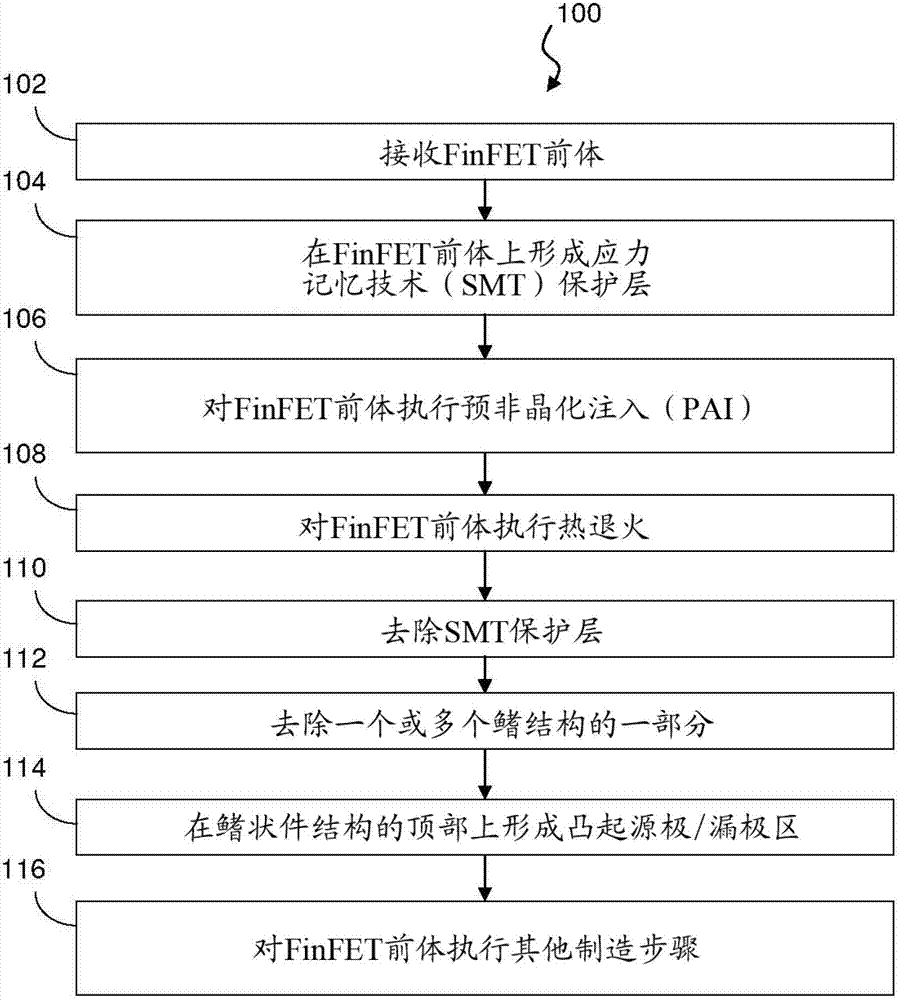
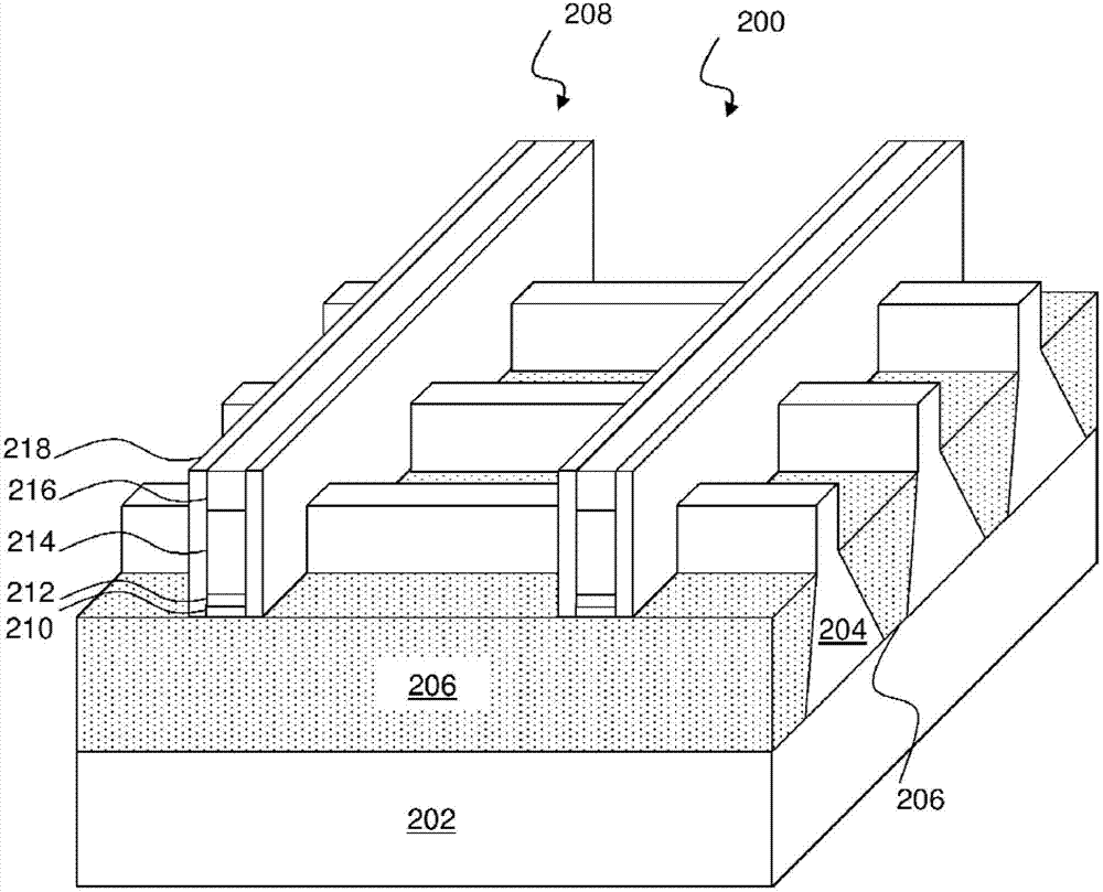
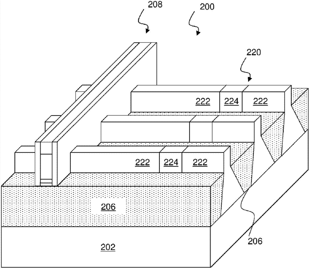
[0035] The present invention relates generally to IC device fabrication and, more particularly, to processes for performing stress memory technology (SMT) on FinFETs and the resulting devices.

[0036] The following disclosure provides a number of different embodiments or examples for implementing different features of the invention. Specific examples of components and arrangements are described below to simplify the present disclosure. Of course, these are examples only and are not intended to be limiting. For example, in the following description a first component formed on or over a second component may include embodiments where the first and second components are in direct contact, and may also include that additional components may be formed between the first and second components , such that the first and second components may not be in direct contact with each other. In addition, the present invention may repeat reference numerals and / or letters in various instances. ...


PUM


Abstract

A method for performing a stress memorization technique (SMT) a FinFET and a FinFET having memorized stress effects including multi-planar dislocations are disclosed. An exemplary embodiment includes receiving a FinFET precursor with a substrate, a fin structure on the substrate, an isolation region between the fin structures, and a gate stack over a portion of the fin structure. The gate stack separates a source region of the fin structure from a drain region of the fin structure and creates a gate region between the two. The embodiment also includes forming a stress-memorization technique (SMT) capping layer over at least a portion of each of the fin structures, isolation regions, and the gate stack, performing a pre-amorphization implant on the FinFET precursor by implanting an energetic doping species, performing an annealing process on the FinFET precursor, and removing the SMT capping layer. The invention further provides dislocation SMT for the FinFET device.

Description

technical field [0001] The invention relates to the field of semiconductors, and more specifically, the invention relates to a dislocation SMT for FINFET devices. Background technique [0002] As the semiconductor industry evolves to pursue higher device density, higher performance, and lower cost nanotechnology process nodes, challenges from manufacturing and design issues drive the development of 3D designs such as Fin Field Effect Transistors (FinFETs) . Exemplary FinFETs are fabricated with thin "fins" (or fin structures) extending from a substrate, eg, etched into a silicon layer of the substrate. The channel of the FET is formed in the vertical fin. A gate is provided over (eg, surrounding) the fin. It is beneficial to place the gates on both sides of the channel, allowing gate control of the channel from both sides. Advantages of FinFET devices include reduced short channel effects and higher current flow. [0003] Due to the inherent complexity of non-planar dev...

Claims


Application Information

Patent Timeline
Patent Type & Authority Applications(China)
IPC IPC(8): H01L21/336H01L29/78
CPCH01L29/785H01L29/78H01L29/7847H01L29/66795H01L29/7853H01L29/7851H01L21/0228H01L21/265H01L21/324H01L21/02299H01L29/0847H01L29/7848
Inventor 罗文政张胜杰
Owner TAIWAN SEMICON MFG CO LTD
Why Eureka
Try Eureka