

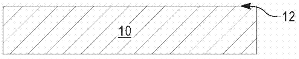
Bilayer gate dielectric with low equivalent oxide thickness for graphene devices
A graphene layer, double-layer gate technology, applied in semiconductor devices, semiconductor/solid-state device manufacturing, nanotechnology for materials and surface science, etc., can solve problems such as expensive equipment
- Summary
- Abstract
- Description
- Claims
- Application Information
AI Technical Summary
Problems solved by technology
Method used
Image

Examples
example 1
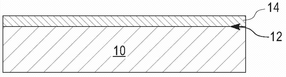
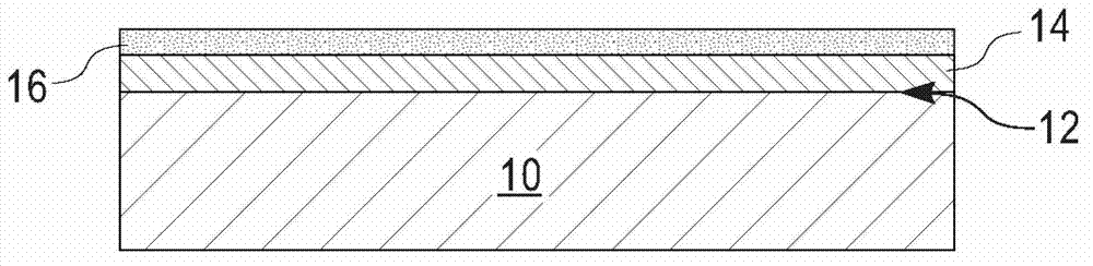
[0064] This example provides a graphene-containing structure comprising an underlying graphene layer with overlying HfO 2 between SiN layers. The structure is prepared by first providing a SiC base substrate and then epitaxially growing a graphene layer on the uppermost surface of the base substrate. The graphene layer is formed using the annealing treatment mentioned in the above detailed description of the present disclosure. After disposing a graphene layer on top of the SiC base substrate, a 2 nm thick stretched SiN layer was formed by PECVD at 400°C. Next, a 10 nm thick HfO was formed by ALD on top of the SiN layer 2 layer.
[0065] Figure 9A is an actual AFM height image of the structure after forming a SiN layer on top of the graphene layer according to this example of the present disclosure. The Z scale in nm is shown on the right. The different terrain heights of this image are indicated by the different shading corresponding directly to the shaded z-scale bar ...
example 2
[0070] This example provides a graphene-containing structure where HfO 2 layer is formed directly on the uppermost surface of the graphene layer. The structure is prepared by first providing a SiC base substrate and then epitaxially growing a graphene layer on the uppermost surface of the base substrate. The graphene layer is formed using the annealing treatment mentioned in the above detailed description of the present disclosure. After disposing a graphene layer on top of the SiC base substrate, a 10-nm-thick HfO layer was formed directly on the uppermost surface of the graphene layer by ALD. 2 layer.
[0071] Figure 13 is the direct formation of HfO on top of the graphene layer according to the present example of the disclosure 2 Actual AFM height image of the structure after the layer. The Z scale is shown on the right. Figure 14 is an example of HfO formed directly on top of a graphene layer 2 Cross-sectional AFM image of layer roughness.
[0072] SEM and AFM pr...
PUM
| Property | Measurement | Unit |
|---|---|---|
| thickness | aaaaa | aaaaa |
| thickness | aaaaa | aaaaa |
| thickness | aaaaa | aaaaa |
Abstract
Description
Claims
Application Information