Method of forming HfSiN metal for n-FET applications

a technology of hfsin metal and nfet, which is applied in the field of forming hfsin metal for nfet applications, complementary metal oxide semiconductors (cmos), can solve the problems of further degradation of device performance, limiting the choice of materials, and using a polysilicon gate, so as to improve the quality of the film and the effect of higher resistivity

Inactive Publication Date: 2006-07-13
GLOBALFOUNDRIES INC
View PDF12 Cites 18 Cited by
  • Summary
  • Abstract
  • Description
  • Claims
  • Application Information

AI Technical Summary

Benefits of technology

[0018] In accordance with the present invention, the Si source diluted with He, which limits the Si source reactivity, improves the quality of the film. The resistivities of the HfSiN film can vary depending on the concentration of the process gases. Typically, the higher the nitrogen and / or Si concentrations, the higher the resistivity.

Problems solved by technology

However, there are also some problems associated with using a polysilicon gate.
Another problem with polySi gates is that the dopant in the polySi gate, such as boron, can easily diffuse through the thin gate dielectric causing further degradation of the device performance.
Gate stack reactions occur during this high temperature anneal limiting the choice of materials.
Metal compounds may be more stable, but still have problems with targeting the right workfunction.
Furthermore, it appears that the inversion thickness scability is somewhat limited using TaSiN.

Method used


Image

  • Method of forming HfSiN metal for n-FET applications
  • Method of forming HfSiN metal for n-FET applications
  • Method of forming HfSiN metal for n-FET applications

Examples


example

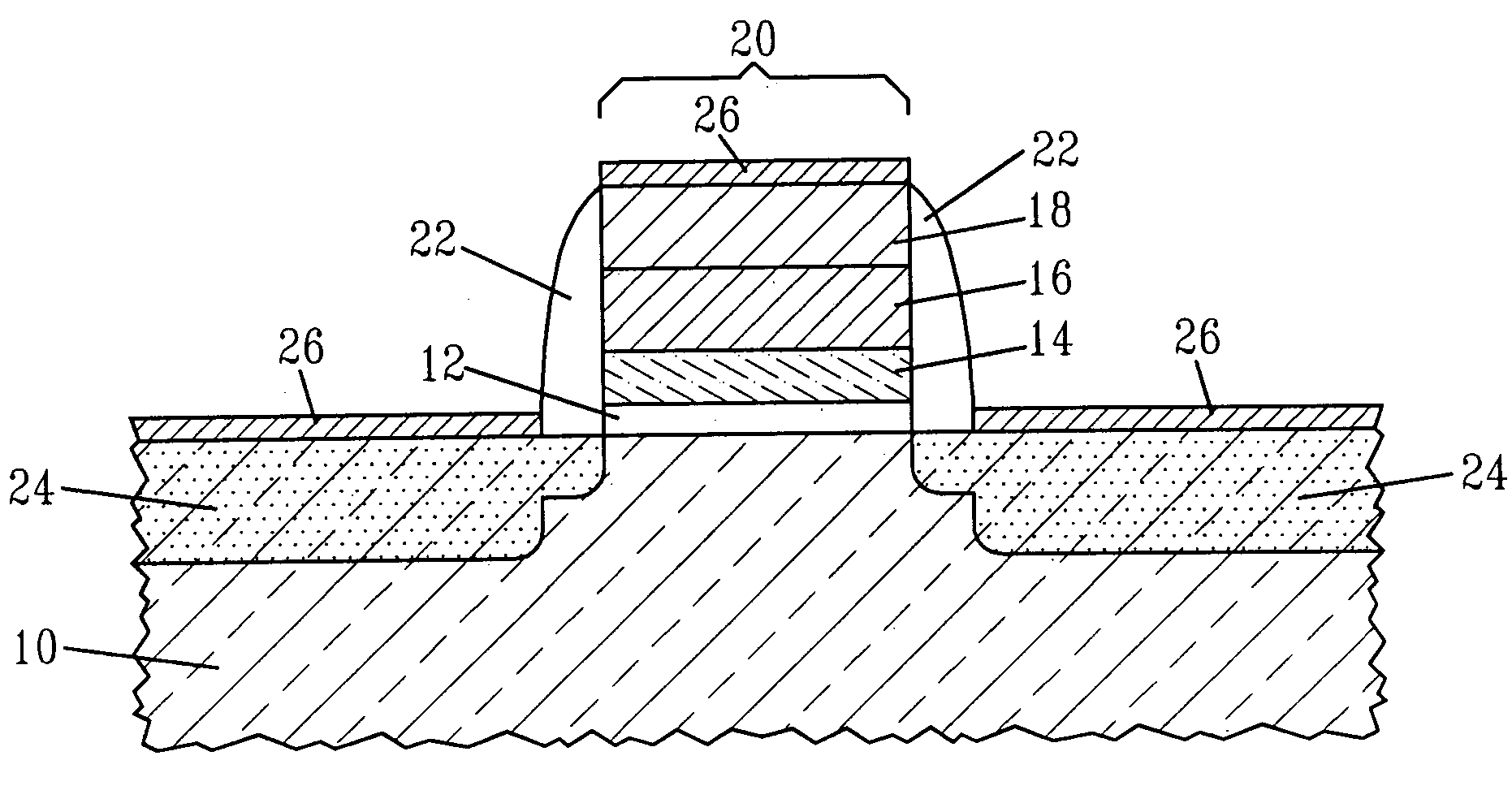
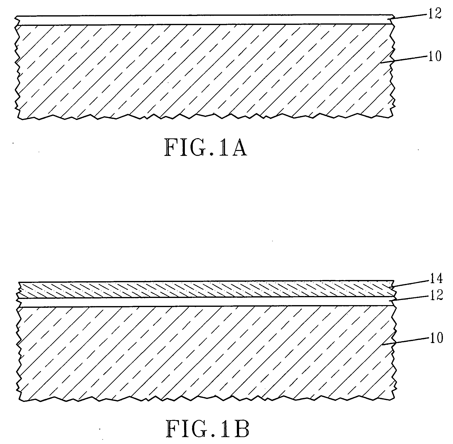
[0062] In this example, a HfSiN / HfO2 / SiO2 stack was formed on a surface of a Si wafer. The SiO2 interfacial layer was formed by oxidation of the Si wafer. The thickness of the SiO2 interfacial layer was about 1 nm. A HfO2 dielectric having a thickness of about 3 nm was then formed on the SiO2 interfacial layer by ALD. The HfSiN layer was then formed by providing a Hf target and an atmosphere comprising Ar / N2 / SiH4 (2% in He) in which flow ratio of Ar:N2:SiH4 (2% in He) was 20:10:20 sccm, respectively. The HfSiN layer had a thickness of about 40 nm. After providing the stack, the stack was subjected to a 1000° C. anneal, followed by a forming gas anneal that was performed at 450° C. For comparison, a TaSiN compound metal was formed about a similar HfO2 / SiO2 stack. FIG. 3 shows the CV characteristics at 10 kHz of these stacks on a n-substate. Note that the workfunction for the stack containing HfSiN was about 4.3 eV which is typical for a NMOS device, while the TaSiN-containing stack h...


PUM

PropertyMeasurementUnit
thicknessaaaaaaaaaa
dielectric constantaaaaaaaaaa
thicknessaaaaaaaaaa

Abstract

A compound metal comprising HfSiN which is a n-type metal having a workfunction of about 4.0 to about 4.5, preferably about 4.3, eV which is thermally stable on a gate stack comprising a high k dielectric and an interfacial layer. Furthermore, after annealing the stack of HfSiN/high k dielectric/interfacial layer at a high temperature (on the order of about 1000° C.), there is a reduction of the interfacial layer, thus the gate stack produces a very small equivalent oxide thickness (12 Å classical), which cannot be achieved using TaSiN.

Description

FIELD OF THE INVENTION [0001] The present invention relates to a semiconductor device and a method of fabricating the same. More particularly, the present invention relates to a complementary metal oxide semiconductor (CMOS) device which includes a thermally stable n-type metal on a high dielectric constant, k / interfacial layer stack. The present invention also provides a process for forming the thermally stable n-type metal which can be integrated with a CMOS processing flow. BACKGROUND OF THE INVENTION [0002] In standard CMOS devices, polysilicon is typically the standard gate material. The technology of fabricating CMOS devices using polysilicon gates has been in a constant state of development, and is now widely used in the semiconductor industry. One advantage of using polysilicon gates is that they can sustain high temperatures. However, there are also some problems associated with using a polysilicon gate. For example, due to the poly-depletion effect and relative high electr...

Claims


Application Information

Patent Timeline
Patent Type & Authority Applications(United States)
IPC IPC(8): H01L29/94
CPCH01L21/28088H01L29/4966H01L29/513H01L29/517H01L29/665H01L29/6659
Inventor CALLEGARI, ALESSANDRO C.FRANK, MARTIN M.JAMMY, RAJARAOLACEY, DIANNE L.MCFEELY, FENTON R.ZAFAR, SUFI
Owner GLOBALFOUNDRIES INC
Why Eureka
Try Eureka