Metal oxynitride as a pFET material

a technology of metal oxynitride and pfet, which is applied in the direction of semiconductor devices, basic electric elements, electrical equipment, etc., can solve the problems of further degradation of device performance, single metals not thermally stable on a high, and use of polysilicon gates

Active Publication Date: 2007-06-21
GLOBALFOUNDRIES US INC
View PDF9 Cites 23 Cited by
  • Summary
  • Abstract
  • Description
  • Claims
  • Application Information

AI Technical Summary

Benefits of technology

[0008] Furthermore, the MOxNy metal compound of the present invention when very thin (equal to or less than 30 nm) is a very efficient oxygen diffusion barrier at 1000° C. allowing very aggressive equivalent oxide thickness (EOT) and inversion layer thickness scaling below 14 Å in a p-metal oxide semiconductor (pMOS) device. Moreover, the MOxNy metal compound does not exhibit any significant carbon diffusion in the interlayers as may be the case with metal carbides.

Problems solved by technology

However, there are also some problems associated with using a polysilicon gate.
Another problem with polySi gates is that the dopant in the polySi gate, such as boron, can easily diffuse through the thin gate dielectric causing further degradation of the device performance.
Although such technology has been suggested, single metals are not thermally stable on a high k (dielectric constant greater than about 4.0) / interfacial layer gate stack.
For example, tungsten, W, and rhenium, Re have stability problems at 1000° C. Tungsten shows interfacial SiO2 regrowth at 4-5 Å after 1000° C., 5 second anneal limiting device scaling and Re is not stable on a high k gate stack, leading to device (mobility) degradation.
Also, it has been reported that high electron mobilities are obtained when performing a high temperature anneal.
However, most of the work reported on TiN shows that TiN is a mid-gap material which may have limited device performance.
While metal carbides are electrically stable at 1000° C. and pFET behavior is maintained, carbon diffusion may occur in the interlayers which may, in turn, contribute to carbon contamination.

Method used


Image

  • Metal oxynitride as a pFET material
  • Metal oxynitride as a pFET material
  • Metal oxynitride as a pFET material

Examples


example

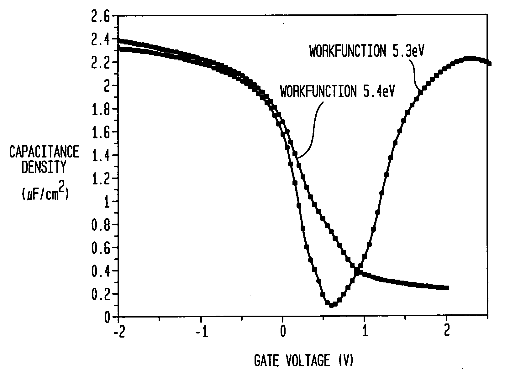
[0060] In this example, a TiOxNy / HfO2 / SiO2 stack was formed on a surface of a p-type Si wafer and an n-type Si wafer. The SiO2 interfacial layer was formed by oxidation of the Si wafer. The thickness of the SiO2 interfacial layer was about 1 nm. A HfO2 dielectric having a thickness of about 3 nm was then formed on the SiO2 interfacial layer by MOCVD. The TiOxNy layer was then formed by sputtering in an Ar / N2 atmosphere from a Ti target. The sputtering was performed in a long throw system (6″ separation between the substrate and target) and, as such, 25 atomic percent oxygen was incorporated into the Ti metal from a pre-sputter background pressure of about 1×10⁻⁷ Torr. The TiOxNy layer had a thickness of about 30 nm.

[0061] After providing the stack, the stack was subjected to a rapid thermal anneal at 1000° C. in N2 and a forming gas at 450° C. anneal was separately performed. FIG. 3 shows the CV characteristics of this stack on both the n-type substrate and the p-type substrate. Th...


PUM

PropertyMeasurementUnit
workfunctionaaaaaaaaaa
pressureaaaaaaaaaa

Abstract

A compound metal comprising MOxNy which is a p-type metal having a workfunction of about 4.75 to about 5.3, preferably about 5, eV that is thermally stable on a gate stack comprising a high k dielectric and an interfacial layer is provided as well as a method of fabricating the MOxNy compound metal. Furthermore, the MOxNy metal compound of the present invention is a very efficient oxygen diffusion barrier at 1000° C. allowing very aggressive equivalent oxide thickness (EOT) and inversion layer thickness scaling below 14 Å in a p-metal oxide semiconductor (PMOS) device. In the above formula, M is a metal selected from Group IVB, VB, VIB or VIIB of the Periodic Table of Elements, x is from about 5 to about 40 atomic % and y is from about 5 to about 40 atomic %.

Description

FIELD OF THE INVENTION [0001] The present invention relates to a semiconductor device and a method of fabricating the same. More particularly, the present invention relates to a complementary metal oxide semiconductor (CMOS) device which includes a thermally stable p-type metal oxynitride (e.g., MOxNy) compound on a high dielectric constant, k / interfacial layer stack. The present invention also provides a process for forming the thermally stable p-type compound metal which can be integrated within a CMOS processing flow. BACKGROUND OF THE INVENTION [0002] In standard CMOS devices, polysilicon is typically the standard gate material. The technology of fabricating CMOS devices using polysilicon gates has been in a constant state of development, and is now widely used in the semiconductor industry. One advantage of using polysilicon gates is that they can sustain high temperatures. However, there are also some problems associated with using a polysilicon gate. For example, due to the p...

Claims


Application Information

Patent Timeline
Patent Type & Authority Applications(United States)
IPC IPC(8): H01L29/78H01L21/336
CPCH01L21/28088H01L21/823828H01L29/4908H01L29/4966H01L29/513H01L29/517H01L29/518
Inventor CALLEGARI, ALESSANDRO C.GRIBELYUK, MICHAEL A.NARAYANAN, VIJAYPARUCHURI, VAMSI K.ZAFAR, SUFI
Owner GLOBALFOUNDRIES US INC
Why Eureka
Try Eureka