Test circuit and test method for pixel array, display panel and display

A technology for testing circuits and pixel arrays, applied in static indicators, instruments, identification devices, etc., can solve the problems of leakage current of display devices, many IC pads, and corresponding port requirements of IC chips, etc., so as to avoid leakage current. and the effect of the short circuit problem

Active Publication Date: 2013-08-28
XIAMEN TIANMA MICRO ELECTRONICS
View PDF5 Cites 11 Cited by
  • Summary
  • Abstract
  • Description
  • Claims
  • Application Information

AI Technical Summary

Problems solved by technology

[0004] The purpose of the present invention is to provide a test circuit for a pixel array, a test method, a display panel, and a display, so as to solve the problem that the test circuit in the prior art needs more IC pads for input signals, and then the corresponding ports of the IC chips also need more , and after the test, the test circuit cannot be closed and is in a suspended state, which may easily cause leakage or short circuit of the display device

Method used


Image

  • Test circuit and test method for pixel array, display panel and display
  • Test circuit and test method for pixel array, display panel and display
  • Test circuit and test method for pixel array, display panel and display

Examples


Embodiment Construction

[0034] The implementation process of the embodiment of the present invention will be described in detail below in conjunction with the accompanying drawings.

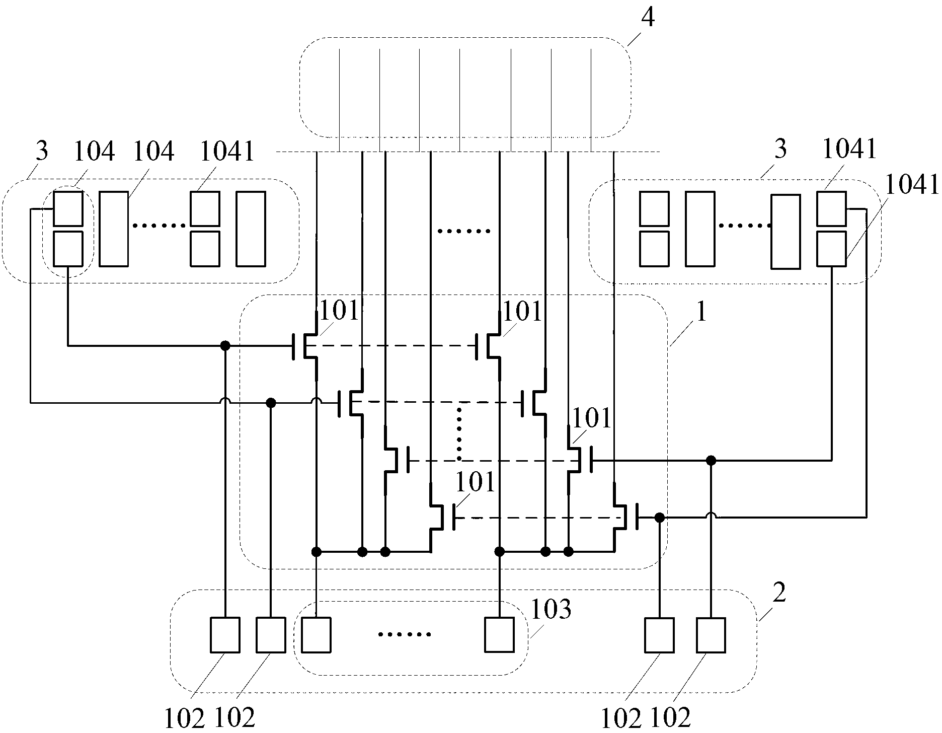
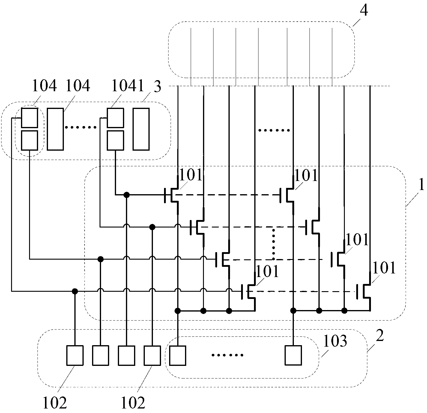
[0035] Embodiment 1 of the present invention provides a test circuit for a pixel array, such as Figure 1A As shown, for the convenience of description, the test circuit is divided into a switch circuit area 1, a test pad area 2, an IC pad area 3, and a pixel array area 4, wherein the pixel array area 4 includes several data lines, including:

[0036] The switch circuit area 1 includes M thin film field effect transistor MOS switches 101, and the source / drain of each MOS switch 101 is electrically connected to the data line of the pixel array;

[0037] Such as Figure 1A In the preferred embodiment shown, the number of thin film field effect transistor MOS switches is the same as the number of data lines of the pixel array, and the data lines of the pixel array are electrically connected to the sources / drains of the MOS ...


PUM


Abstract

The invention discloses a test circuit and a test method for a pixel array, a display panel and a display. The test circuit comprises M MOS (metal oxide semiconductor) switches, N first test gaskets, K second test gaskets and P IC (integrated circuit) gaskets, wherein the source electrode / drain electrode of each MOS switch is electrically connected with the data line of the pixel array; the N first test gaskets are used for inputting a test control signal for respectively controlling on and off of M MOS switches; each first test gasket is electrically connected with the grid electrode of at least one MOS switch; the K second test gaskets are used for inputting a data signal; each second test gasket is electrically connected with the source electrode / drain electrode of at least one MOS switch; at least one IC gasket comprises at least two sub gaskets; and at least two sub gaskets in the IC gasket are respectively electrically connected with the grid electrodes of the MOS switches of the same number in a one-one correspondence mode. A plurality of IC gaskets are replaced by sub gaskets contained in IC, and the number of the IC gaskets used for inputting a specified potential to close a switching circuit line is reduced when the switches are respectively controlled.

Description

technical field [0001] The invention relates to the field of liquid crystal display, in particular to a test circuit of a pixel array, a test method, a display panel and a display including the test circuit of the pixel array. Background technique [0002] Due to the continuous progress of display manufacturing technology and the higher requirements of various application fields, high-resolution displays have become an inevitable trend of development, but high-resolution displays, especially for high-resolution liquid crystal displays, correspond to high-resolution It is an increase in the geometric multiple of pixels, corresponding to more and more data lines. [0003] When testing a high-resolution liquid crystal display, an astonishing number of data lines and signal input pads need to be provided to the test circuit according to the number of pixels. In the prior art, a plurality of switches are usually added to the test circuit to form a switch circuit to reduce the co...

Claims


Application Information

Patent Timeline
IPC IPC(8): G09G3/00G09F9/35
Inventor 夏军周莉
Owner XIAMEN TIANMA MICRO ELECTRONICS
Why Eureka
Try Eureka