Fully-packaged internal insulation semiconductor device

A semiconductor and internal insulation technology, which is applied in semiconductor devices, semiconductor/solid-state device components, electric solid-state devices, etc., can solve problems that affect the reliability of semiconductor devices, affect the heat dissipation performance of semiconductor devices, and increase the risk of overheating of semiconductor devices. To achieve the effect of avoiding leakage and short circuit problems, reducing the risk of overheating, and saving maintenance costs

Inactive Publication Date: 2021-09-17
广东仁懋电子有限公司
View PDF0 Cites 0 Cited by
  • Summary
  • Abstract
  • Description
  • Claims
  • Application Information

AI Technical Summary

Problems solved by technology

[0003] However, most traditional semiconductor devices adopt a semi-encapsulated external insulation structure, which is not only prone to leakage and short circuit problems due to damage to the external insulation layer, but also affects the poor reliability of the semiconductor device, and also affects the heat dissipation performance of the semiconductor device. The overheating risk of the device shortens the service life of the semiconductor device, and it is inconvenient to disassemble after installation, making maintenance and replacement difficult, which inevitably increases the maintenance cost of the semiconductor device

Method used


Image

  • Fully-packaged internal insulation semiconductor device
  • Fully-packaged internal insulation semiconductor device
  • Fully-packaged internal insulation semiconductor device

Examples


Embodiment Construction

[0025] The following will clearly and completely describe the technical solutions in the embodiments of the present invention with reference to the accompanying drawings in the embodiments of the present invention. Obviously, the described embodiments are only some, not all, embodiments of the present invention. Based on the embodiments of the present invention, all other embodiments obtained by those of ordinary skill in the art without creative efforts shall fall within the protection scope of the present invention.

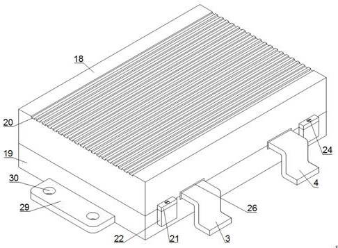
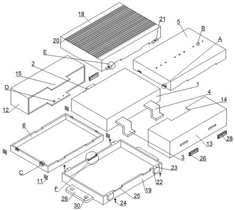
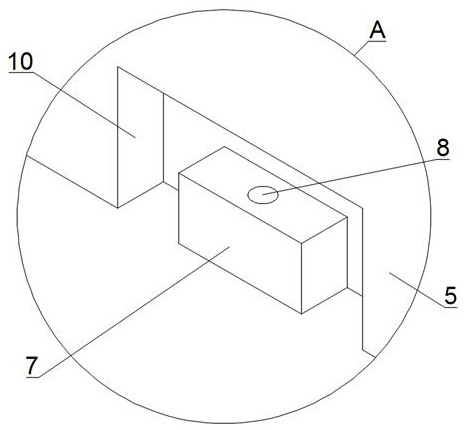
[0026] see Figure 1-8, the present invention provides a technical solution: a fully encapsulated inner insulating semiconductor device, including a semiconductor body 1, a collector pin 2, a base pin 3, an emitter pin 4, a first insulating inner shell 5, a second Two insulating inner shells 6, limiting blocks 7, positioning holes 8, positioning columns 9, limiting slots 10, limiting frames 11, first thermally conductive rubber sleeves 12, second thermally cond...


PUM


Abstract

The invention discloses a fully-packaged internal insulation semiconductor device. The device comprises a semiconductor main body, a collector electrode pin, a base electrode pin, an emitter electrode pin, a first insulation inner shell, a second insulation inner shell, a limiting block, a positioning hole, a positioning column, a limiting groove, a limiting frame, a first heat conduction rubber sleeve, a second heat conduction rubber sleeve, a mortise, a tenon part, a groove, a convex block, a first insulation outer shell, a second insulation outer shell, a heat dissipation grid groove, a connecting lug plate, a connecting column, a connecting screw hole and a connecting screw. A sleeve hole, a rubber sleeve, a frame groove, a convex frame, a mounting plate and a mounting hole; according to the invention, a fully-packaged internal insulation structure is adopted, so that the problems of electric leakage and short circuit of the semiconductor device after the insulation layer is damaged are avoided. The working reliability of the semiconductor device is improved, the heat dissipation performance of the semiconductor device is improved, the overheating risk of the semiconductor device is reduced, and the service life of the semiconductor device is prolonged. The device is easy to disassemble after being installed. The maintenance and replacement are convenient, and maintenance cost of the semiconductor device is saved.

Description

technical field [0001] The invention relates to the technical field of semiconductor devices, in particular to a fully encapsulated internal insulating semiconductor device. Background technique [0002] A semiconductor device is an electronic device whose conductivity is between a good conductor and an insulator. It uses the special electrical properties of semiconductor materials to complete specific functions. It can be used to generate, control, receive, transform, amplify signals and perform energy conversion. The semiconductor material of semiconductor devices is silicon, germanium or gallium arsenide, which can be used as rectifiers, oscillators, light emitters, amplifiers, photometers and other equipment. In order to distinguish them from integrated circuits, they are sometimes called discrete devices. [0003] However, most traditional semiconductor devices adopt a semi-encapsulated external insulation structure, which is not only prone to leakage and short circuit ...

Claims


Application Information

Patent Timeline
Patent Type & Authority Applications(China)
IPC IPC(8): H01L23/31H01L23/367H01L23/10
CPCH01L23/3121H01L23/367H01L23/10
Inventor 仇亮窦静
Owner 广东仁懋电子有限公司
Why Eureka
Try Eureka