A kind of processing method after silicon wafer rie texturing
A processing method and silicon wafer technology, which is applied in the manufacture of semiconductor/solid-state devices, electrical components, circuits, etc., can solve the problems of the decline in the failure rate of silicon wafers, and achieve the effect of improving efficiency and sufficient cleaning
- Summary
- Abstract
- Description
- Claims
- Application Information
AI Technical Summary
Problems solved by technology
Method used
Image
Examples
Embodiment Construction
[0022] The following disclosure provides many different embodiments or examples for implementing different structures of the present invention. To simplify the disclosure of the present invention, components and arrangements of specific examples are described below. Furthermore, the present invention may repeat reference numerals and / or letters in different instances. This repetition is for the purpose of simplicity and clarity and does not in itself indicate a relationship between the various embodiments and / or arrangements discussed. It should be noted that components illustrated in the figures are not necessarily drawn to scale. Descriptions of well-known components and processing techniques and processes are omitted herein to avoid unnecessarily limiting the present invention.
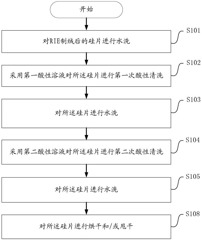
[0023] refer to figure 1 , figure 1 Shown is a schematic flow chart of a specific embodiment of a method for treating a silicon wafer after RIE texturing according to the present invention.
...
PUM
 Abstract
Description
Claims
Application Information

