Check patentability & draft patents in minutes with Patsnap Eureka AI!

Manufacturing method of thin film transistor (TFT) array substrate and TFT array substrate

A technology of an array substrate and a manufacturing method, which is applied in the field of flat panel display, can solve the problems of long period of reticle design, development and production, high cost, rising production cost, etc.

Active Publication Date: 2013-09-04
SHANGHAI AVIC OPTOELECTRONICS
View PDF6 Cites 5 Cited by
  • Summary
  • Abstract
  • Description
  • Claims
  • Application Information

AI Technical Summary

Problems solved by technology

As we all know, the design, development and production cycle of masks is long and expensive, and after each set of masks enters the production site, it needs to be maintained and stored accordingly, that is to say, each additional set of masks will increase the production cost. rise

Method used


Image

  • Manufacturing method of thin film transistor (TFT) array substrate and TFT array substrate
  • Manufacturing method of thin film transistor (TFT) array substrate and TFT array substrate
  • Manufacturing method of thin film transistor (TFT) array substrate and TFT array substrate

Examples


Embodiment Construction

[0050] In order to make the purpose, technical solution and advantages of the present invention more clear, the following will be further described in detail in conjunction with the accompanying drawings.

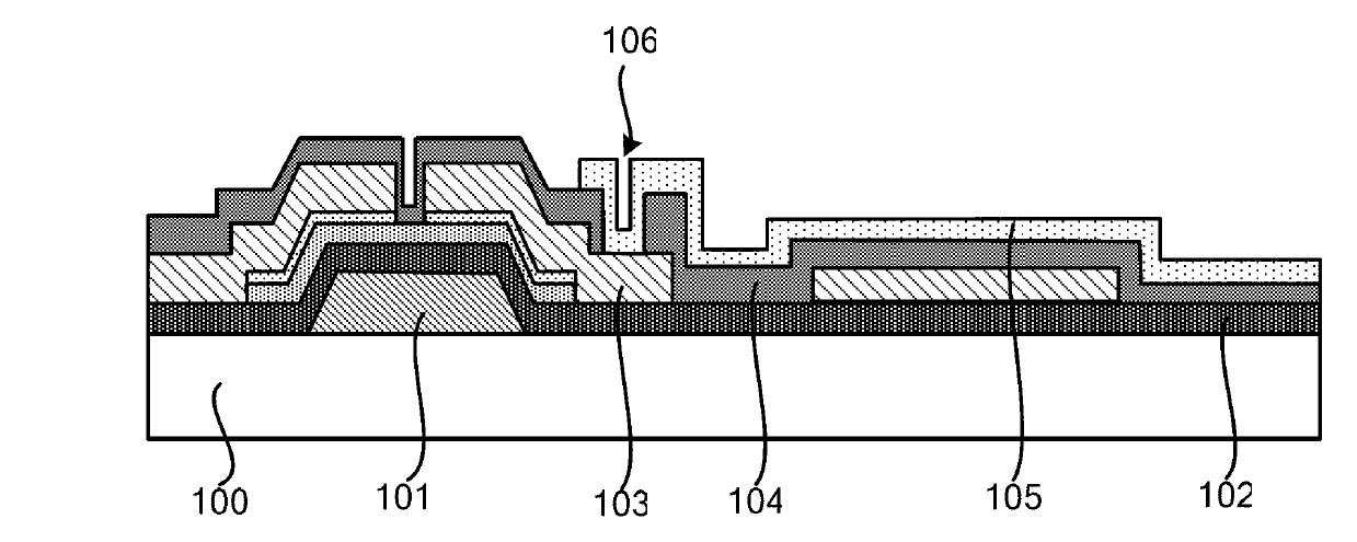
[0051] image 3 It is a top view of a TFT array substrate according to an embodiment of the present invention. Such as image 3 As shown, a TFT array substrate 200 according to an embodiment of the present invention includes a substrate 201 , and the substrate 201 includes a display area 202 and a peripheral area 203 surrounding the display area 202 . A plurality of thin film transistors 204 (Thin Film Transistor, TFT) are included in the display area 203 . Applying an amorphous silicon gate driver integrated with an active matrix (amorphous silicon gate, ASG) technology, a gate drive circuit 205 is provided in the peripheral area 203, and the gate drive circuit 205 can be used to replace a gate drive IC, so that the display becomes lighter.

[0052] Attached below Fi...


PUM


Abstract

The invention discloses a manufacturing method of a thin film transistor (TFT) array substrate and a TFT array substrate. The manufacturing method of the TFT array substrate comprises the following steps that (1) a substrate is provided; (2) lithography is carried out to a first metal layer on the substrate by using a first mask template; (3) lithography is carried out to a first insulation layer by using a second mask template to form a first through hole and a second through hole; (4) lithography is carried out to a second metal layer by using a third mask template; (5) lithography is carried out through the second mask template to form a third through hole and a fourth through hole; and (6) lithography is carried out to a transparent electrode layer by using a fourth mask template to form transparent electrode patterns. When the TFT array substrate which adopts an access security gateway (ASG) technology is manufactured, apart from the four mask templates, a fifth mask template is also needed to form a semi-conductor active layer; and a total of five mask templates are required, and compared with the prior art in which six mask templates are required, a mask template is saved, and the production cost is reduced.

Description

technical field [0001] The invention relates to flat panel display technology, in particular to a manufacturing method of a TFT array substrate and the TFT array substrate. Background technique [0002] Thin Film Transistor Liquid Crystal Display (TFT-LCD) is widely used in mobile phones, handheld computers (Personal Digital Assistant, PDA) and other portable electronic products. Driven by market competition, thin-film transistor liquid crystal displays with lighter weight, better display effect and lower price are becoming more and more popular. The technology of integrating the amorphous silicon gate driver with the active matrix (amorphous silicon gate, ASG) can reduce the TFT-LCD display by one driver IC, which can effectively make the display screen lighter, reduce the cost, and increase the display capacity. reliability. Therefore, in recent years, ASG technology has gradually become a hot spot in development and research. [0003] An array substrate using ASG tech...

Claims


Application Information

Patent Timeline
Patent Type & Authority Applications(China)
IPC IPC(8): H01L21/77H01L27/12H01L29/786
Inventor 周思思
Owner SHANGHAI AVIC OPTOELECTRONICS
Features
  • R&D
  • Intellectual Property
  • Life Sciences
  • Materials
  • Tech Scout
  • Unparalleled Data Quality
  • Higher Quality Content
  • 60% Fewer Hallucinations
Learn More