Memory resisting layer and memory resistor
A memristor and resistive layer technology, applied in the field of microelectronics and semiconductor technology, can solve the problems of small discreteness of electrical characteristic parameters, large working voltage and working current of the memristor, and achieve superior performance, reduce operating voltage and operation. Current, the effect of improving dispersion
- Summary
- Abstract
- Description
- Claims
- Application Information
AI Technical Summary
Problems solved by technology
Method used
Image

Examples
Embodiment 1
[0033] A memristive layer described in this embodiment includes a main layer and an auxiliary layer;
[0034] the auxiliary layer is located on top of the main layer;
[0035] the thickness of the main layer is greater than the thickness of the auxiliary layer;
[0036] The main layer is made of metal oxide A with resistive switching properties x1 o y1 constitute;
[0037] The auxiliary layer is made of metal oxide B x2 o y2 constitute;
[0038] Among them, x1, x2, y1, and y2 are the ratios of elements related to chemical valence.
Embodiment 2
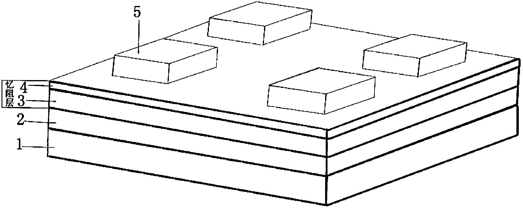
[0040] Such as figure 2 As shown, a memristive layer described in this embodiment includes a main layer 3 and an auxiliary layer 4 . Wherein, the auxiliary layer 4 is located above the main layer 3; and the thickness of the main layer 3 is greater than the thickness of the auxiliary layer 4; the main layer 3 is made of metal oxide A with resistive properties x1 o y1 Composition; auxiliary layer 4 is made of metal oxide B x2 o y2 constitute. Among them, x1, x2, y1, and y2 are the ratios of elements related to chemical valence.
[0041] Main Layer 3 Metal Oxide A x1 o y1 and auxiliary layer 4 of metal oxide B x2 o y2 The metal elements have different valence states.
[0042] When the main layer 3 metal oxide A x1 o y1 for HfO 2 , then the metal oxide B of the auxiliary layer 4 x2 o y2 Can be Al 2 o 3 、Gd 2 o 3 or Ta 2 o 5 ; when the metal oxide A of the main layer 3 x1 o y1 for Al 2 o 3 , then the metal oxide B of the auxiliary layer 4 x2 o y2 Can be T...
Embodiment 3
[0047] A memristor described in this embodiment includes a bottom electrode layer, the above-mentioned memristor layer and a top electrode layer;
[0048] The oxygen storage capacity of the top electrode layer material is greater than the oxygen storage capacity of the bottom electrode layer material;
[0049] The bottom electrode layer and the top electrode layer are used for electrical connection with an external operating circuit;
[0050] The memristive layer is located between the bottom electrode layer and the top electrode layer.
[0051] The memristor also includes a substrate underlying the underlying bottom electrode layer.
PUM
 Abstract
Description
Claims
Application Information
 - R&D
- Intellectual Property
- Life Sciences
- Materials
- Tech Scout
- Unparalleled Data Quality
- Higher Quality Content
- 60% Fewer Hallucinations
Browse by: Latest US Patents, China's latest patents, Technical Efficacy Thesaurus, Application Domain, Technology Topic, Popular Technical Reports.
© 2025 PatSnap. All rights reserved.Legal|Privacy policy|Modern Slavery Act Transparency Statement|Sitemap|About US| Contact US: help@patsnap.com