Liquid crystal display

A technology of liquid crystal display device and display area, which is applied in the direction of instruments, semiconductor devices, optics, etc., and can solve problems such as horizontal stripes and poor display effect

Active Publication Date: 2013-09-11
BEIHAI HKC OPTOELECTRONICS TECH CO LTD
View PDF3 Cites 7 Cited by
  • Summary
  • Abstract
  • Description
  • Claims
  • Application Information

AI Technical Summary

Problems solved by technology

[0004] In view of this, the object of the present invention is to provide a liquid crystal display device to solve the problem of horizontal stripes and poor display effect in the existing liquid crystal display device

Method used


Image

  • Liquid crystal display
  • Liquid crystal display
  • Liquid crystal display

Examples


Embodiment 1

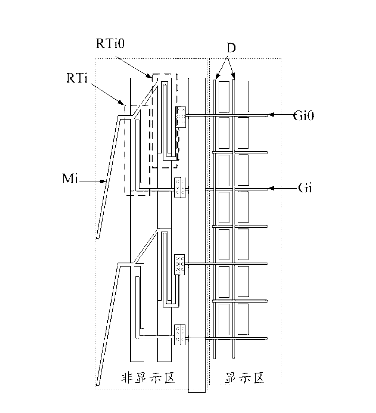
[0033] This embodiment discloses a liquid crystal display device, such as figure 1 As shown, the LCD display includes:

[0034] A thin film transistor substrate, the thin film transistor substrate includes a display area and a non-display area, and a plurality of scanning lines, a plurality of data lines D and a plurality of thin film transistors (not shown in the figure) are arranged in the display area; A plurality of resistance-adjusting thin film transistors and a plurality of peripheral leads are arranged in the display area;

[0035] The peripheral leads are the passages through which external drive signals are introduced into the display area, and the peripheral leads are arranged on the same conductive layer, so the signal delay of the peripheral leads is only related to the resistance of the peripheral leads, and each peripheral lead passes through two The resistance-adjusting thin film transistors are respectively connected to the two scanning lines, while the perip...

Embodiment 2

[0048] This embodiment discloses another liquid crystal display device, which differs from the above embodiments in that:

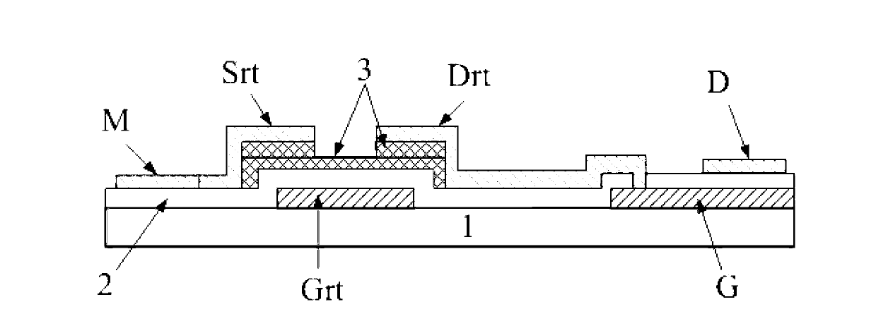
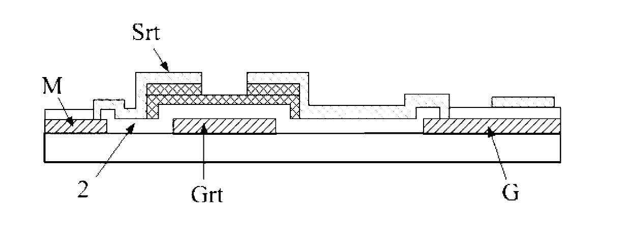
[0049] Such as image 3 As shown, in this embodiment, the peripheral lead M is arranged on the first metal layer together with the scan line G and the gate Grt of the resistance-adjusting thin film transistor, so as to arrange other functional layers on the second metal layer. At this time, the peripheral lead M is electrically connected to the source Srt of the resistance-adjusting thin film transistor through the via hole provided in the gate insulating layer 2 .

Embodiment 3

[0051] This embodiment discloses a manufacturing method of the above-mentioned liquid crystal display device. In the method, the resistance-adjusting thin film transistor and the thin film transistor in the display area are manufactured simultaneously through the same steps.

[0052] Specifically, the method includes:

[0053] A substrate is provided, a first metal layer is formed on the surface of the substrate, and the first metal layer is patterned to form gates of the resistance-adjusting thin film transistors in the display area and scan lines and gates of the thin film transistors in the non-display area.

[0054] Specifically, the substrate is a glass substrate or a substrate of other materials.

[0055] Forming the gates of the resistance-adjusting thin film transistors in the display area and the scan lines and gates of the thin film transistors in the non-display area on the surface of the substrate specifically includes:

[0056] The first metal layer is formed on ...


PUM


Abstract

The invention discloses a liquid crystal display. Peripheral leads of the liquid crystal display are arranged in the same conductive layer, so that the signal delays of the peripheral leads are only related to the resistances of the peripheral leads; each peripheral lead is connected with two scanning lines by two resistance-trimming thin film transistors respectively; the resistance Ri of the ith resistance-trimming thin film transistor is preset to be a fixed value; the resistance of the corresponding peripheral lead is RiL; and the resistance Rn of any other nth resistance-trimming thin film transistor and the resistance RnL of the peripheral lead corresponding to the nth resistance-trimming thin film transistor meet the equation that Rn + RnL are equal to Ri + RiL. The resistance Rn of the nth resistance-trimming thin film transistor can compensate the signal delay of the nth peripheral lead, so that the signal delays of the nth peripheral lead and the ith peripheral lead are the same, finally the signal delays of all the peripheral leads and the signal delay of the ith peripheral lead are the same, the liquid crystal display is prevented from cross grains, and the display effect is improved.

Description

technical field [0001] The invention belongs to the field of liquid crystal display, in particular to a liquid crystal display device. Background technique [0002] The information society increasingly needs thin and portable display devices, and the most mature product at present is a liquid crystal display device (Liquid Crystal Display, LCD). [0003] However, when the existing LCD displays pictures, horizontal stripes often appear, which reduces the display effect of the LCD. Contents of the invention [0004] In view of this, the object of the present invention is to provide a liquid crystal display device to solve the problem of horizontal stripes and poor display effect in the existing liquid crystal display device. [0005] The liquid crystal display device includes: [0006] A thin film transistor substrate, the thin film transistor substrate includes a display area and a non-display area, and a plurality of scanning lines, a plurality of data lines and a plural...

Claims


Application Information

Patent Timeline
Patent Type & Authority Applications(China)
IPC IPC(8): G02F1/1362G02F1/1368H01L27/12
Inventor 梁艳峰
Owner BEIHAI HKC OPTOELECTRONICS TECH CO LTD
Why Eureka
Try Eureka