Electrostatic discharge protection structure and semiconductor equipment
An electrostatic discharge protection and electrostatic discharge wire technology, applied in the field of electrostatic discharge protection structures and semiconductor equipment, can solve problems such as reducing product reliability, degrading components, and increasing maintenance costs, achieving a wide range of applicable locations, small parasitic capacitance, simple structure
- Summary
- Abstract
- Description
- Claims
- Application Information
AI Technical Summary
Problems solved by technology
Method used
Image

Examples
Embodiment 1
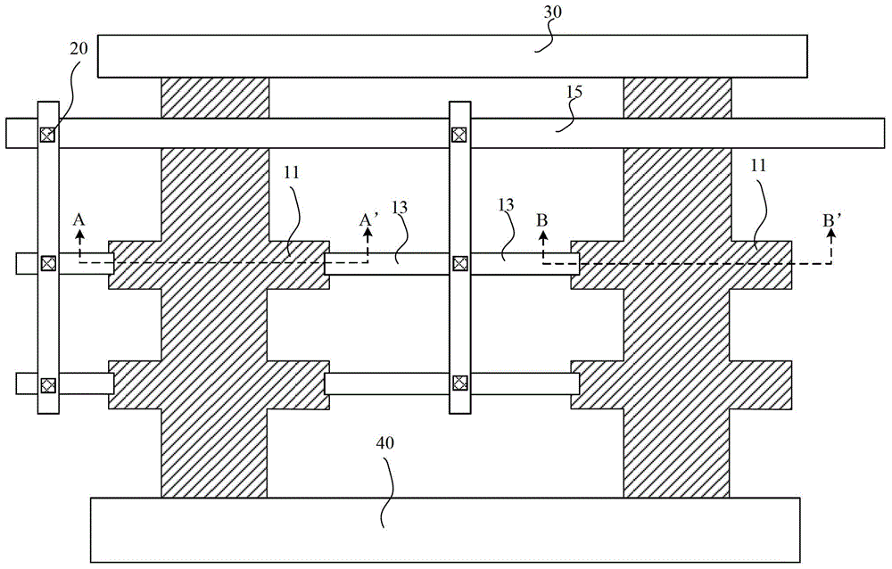
[0061] image 3 Is a cross-sectional view of the electrostatic discharge protection structure in the first embodiment of the present invention, image 3 For the edge figure 1 A cross-sectional view of the ESD protection structure in the A-A' direction, combined with figure 1 with image 3 As shown, the electrostatic discharge protection structure is arranged between the electrostatic sensitive element 30 and the peripheral circuit 40, and the electrostatic discharge protection structure is also connected to the discharge bus; wherein the electrostatic discharge protection structure includes a first interconnect 11 and a passivation layer 12 and at least one electrostatic discharge wire 13, the first interconnection wire 11 electrically connects the electrostatic sensitive element 30 and the peripheral circuit 40, the electrostatic discharge wire 13 and the first interconnection wire 11 pass through the passivation layer 12 Isolated, and the boundary of the electrostatic discharge...
Embodiment 2
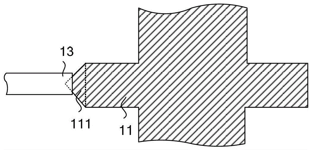
[0067] Figure 4 It is a cross-sectional view of the electrostatic discharge protection structure in the second embodiment of the present invention. Combine Figure 4 On the basis of Embodiment 1, in this embodiment, the electrostatic discharge wire 13 and the first interconnection line 11 are staggered in the longitudinal direction, and the staggered width d2 is greater than 0um and less than or equal to 2.5um, and the staggered width Within this range, d2 can produce a breakdown effect in time when static electricity comes, and then protect the electrostatic sensitive components connected to the electrostatic discharge protection structure.
Embodiment 3
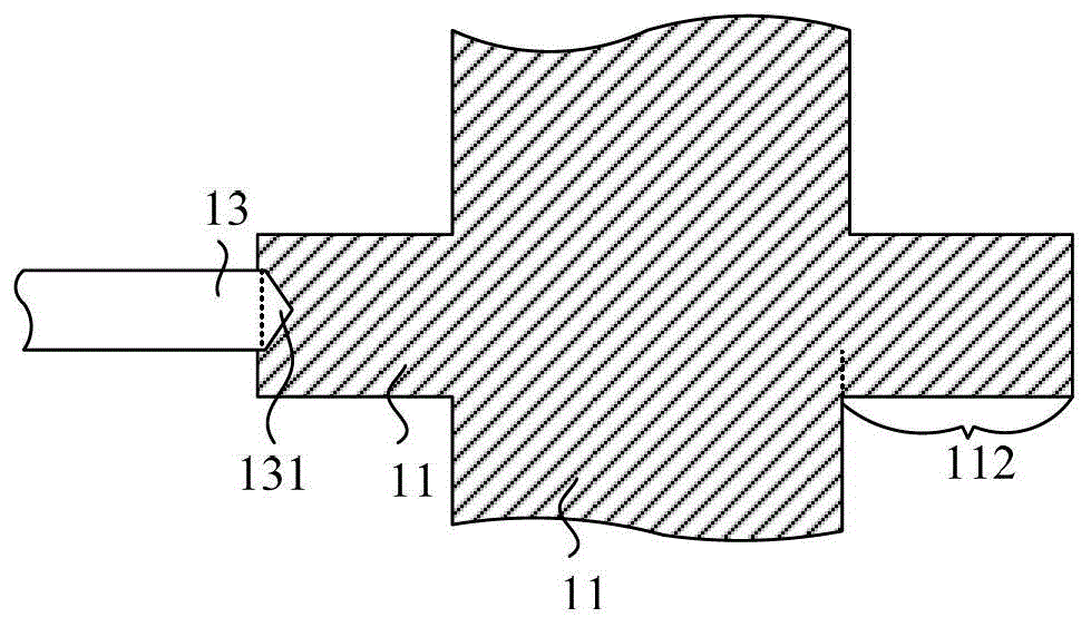
[0069] Figure 5 It is a cross-sectional view of the electrostatic discharge protection structure in the third embodiment of the present invention. Combine Figure 5 On the basis of the first embodiment, the surface where the longitudinal boundary of the electrostatic discharge wire 13 is located coincides with the surface where the longitudinal boundary of the first interconnection line 11 is located. Since the surface of the longitudinal boundary of the electrostatic discharge wire 13 coincides with the surface of the longitudinal boundary of the first interconnect 11, compared with the first and second embodiments, the electrostatic discharge wire 13 is close to the first interconnect. An electrostatic discharge path L can be formed between the vertex angle of the connecting line 11 and the adjacent vertex angle of the first interconnection line 11, and the length of the electrostatic discharge path L ranges from 0.2 μm to 3 μm, so as to be able to be in the passivation layer...
PUM
 Abstract
Description
Claims
Application Information
 - R&D Engineer
- R&D Manager
- IP Professional
- Industry Leading Data Capabilities
- Powerful AI technology
- Patent DNA Extraction
Browse by: Latest US Patents, China's latest patents, Technical Efficacy Thesaurus, Application Domain, Technology Topic.
© 2024 PatSnap. All rights reserved.Legal|Privacy policy|Modern Slavery Act Transparency Statement|Sitemap