Supercharge Your Innovation With Domain-Expert AI Agents!

New Metamaterials and Their Fabrication Process

A manufacturing process and metamaterial technology, applied in the field of metamaterials, can solve the problems of high dielectric constant, signal attenuation, and the inability to use brittle dielectric substrates, etc., and achieve the effect of simple manufacturing process and firm combination

Active Publication Date: 2021-10-19
KUANG CHI INST OF ADVANCED TECH
View PDF11 Cites 0 Cited by
  • Summary
  • Abstract
  • Description
  • Claims
  • Application Information

AI Technical Summary

Problems solved by technology

Therefore, the material of most dielectric substrates can only be the material whose main component is glass fiber, and brittle dielectric substrates, such as ceramics, cannot be used, thus greatly reducing the selectivity of metamaterial dielectric substrates
In addition, the high dielectric constant (ε) and dielectric loss tangent (Tanδ) of metamaterials with glass fibers as dielectric substrates will cause signal attenuation when electromagnetic waves pass through metamaterials made of such dielectric substrates

Method used


Image

  • New Metamaterials and Their Fabrication Process
  • New Metamaterials and Their Fabrication Process

Examples


Embodiment Construction

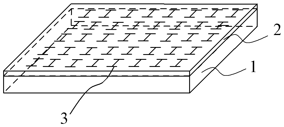
[0022] see figure 1 , the present invention relates to a novel metamaterial, which includes a material sheet, the material sheet includes a dielectric substrate 1, a photosensitive composite layer 2 and a metal layer, and the dielectric substrate 1 can be made of a high molecular polymer material, Made of ceramic material, polytetrafluoroethylene material, ferroelectric material, ferrite material, or ferromagnetic material. In this embodiment, the dielectric substrate 1 is made of materials other than glass fiber epoxy resin, such as polytetrafluoroethylene, so that a lower dielectric constant (ε) and dielectric loss tangent (Tanδ) can be obtained , so as not to cause the problem of signal attenuation when the electromagnetic wave passes through the metamaterial made of the dielectric substrate.

[0023] The photosensitive composite layer 2 is located between the dielectric substrate 1 and the metal layer, and the metal layer is fixed on the dielectric substrate 1 through the...


PUM

PropertyMeasurementUnit
thicknessaaaaaaaaaa
thicknessaaaaaaaaaa

Abstract

The invention relates to a novel metamaterial and its manufacturing process. The material includes at least one material sheet, each material sheet includes a dielectric substrate, a photosensitive composite layer and a metal layer, and the photosensitive composite layer is located on the dielectric substrate. Between the bottom and the metal layer, the metal layer is fixed on the dielectric substrate through the photosensitive composite layer. The manufacturing process of the novel metamaterial includes the following steps: S1, placing the dielectric substrate flat on the workbench; S2, applying a photosensitive material on the dielectric substrate to form a photosensitive composite layer; S3, applying the artificial metal micro The structure covers the photosensitive composite layer to form a metal layer; S4, irradiating the photosensitive composite layer with ultraviolet light to cure the photosensitive composite layer. The manufacturing process of the invention is simple, and various materials can be selected as the dielectric substrate of the metamaterial through the manufacturing process to meet the requirements of electromagnetic characteristics of different metamaterials, and at the same time, the combination of the dielectric substrate and the metal layer is stronger.

Description

technical field [0001] The invention relates to the field of metamaterials, and more specifically, relates to a novel metamaterial and its manufacturing process. Background technique [0002] Metamaterial is a new type of artificial synthetic material with special electromagnetic response characteristics, so it can be widely used in electromagnetic communication and other fields. The metamaterial comprises at least one material sheet layer, each material sheet layer includes a flat plate-shaped dielectric substrate and artificial metal microstructures attached to the dielectric substrate, the dielectric substrate is mainly a glass fiber epoxy resin curing sheet, The artificial metal microstructure is generally a metal wire with a certain geometric pattern such as "I" shape, snowflake shape, split resonator ring and the like. [0003] However, since the existing metamaterial manufacturing process is based on the PCB processing process, that is, a layer of metal foil is depos...

Claims


Application Information

Patent Timeline
Patent Type & Authority Patents(China)
IPC IPC(8): H01Q15/00
Inventor 刘若鹏赵治亚方小伟郭文鹏
Owner KUANG CHI INST OF ADVANCED TECH
Features
  • R&D
  • Intellectual Property
  • Life Sciences
  • Materials
  • Tech Scout
  • Unparalleled Data Quality
  • Higher Quality Content
  • 60% Fewer Hallucinations
Learn More